Micro LED transfer method

A transfer method and LED structure technology, which is applied to electrical components, circuits, semiconductor devices, etc., can solve problems such as difficulty in absorbing successfully, and achieve the effect of improving the transfer success rate and improving the problem of membrane breakage

Inactive Publication Date: 2019-05-24
NANJING CEC PANDA LCD TECH
View PDF3 Cites 18 Cited by
  • Summary
  • Abstract
  • Description
  • Claims
  • Application Information

AI Technical Summary

Problems solved by technology

Since the conventional method is to use the suction head to absorb the LED, but there is a thick metal layer at the bottom, the metal at the bottom needs to be torn off by a strong suction force before transferring
Therefore, it is necessary to pull and break the bottom metal, and a large electrostatic suction force is required to absorb the bottom metal, or even if a large electrostatic suction force is used, it is difficult to successfully absorb
[0003] Therefore, the disadvantage of the existing conventional technology is that a thicker metal is required as a buffer layer for laser peeling stress relief, and at the same time, it is necessary to use suction to break the metal layer during transfer.

Method used


Image

  • Micro LED transfer method
  • Micro LED transfer method
  • Micro LED transfer method

Examples


Embodiment

[0044] This embodiment is a transfer method of micro-LEDs, such as Figure 1 to Figure 12 shown.

[0045] The transfer method includes at least the following steps:

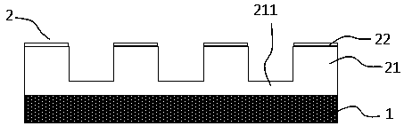
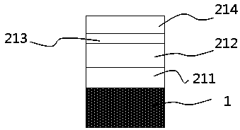
[0046] S1, such as figure 1 As shown, an epitaxial structure is formed on a substrate 1, and after etching (preferably half etching) the epitaxial structure, an array of LED structures 2 is formed on the substrate 1, figure 2 Shown is a partial structural schematic diagram of each LED structure 2 .

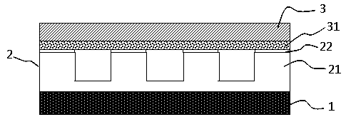
[0047] S2, such as image 3 As shown, after the LED structure 2 in step S1 is transferred to the first transient substrate 3, as Figure 4 As shown, peel off the substrate 1, as Figure 5 As shown, the LED structure 2 and the first transient substrate 3 are turned over together, so that the LED structure 2 is on the top and the first transient substrate 3 is on the bottom.

[0048] S3, such as Image 6 As shown, the LED structure 2 in step S2 is etched again and a plurality of separated LEDs 4 are formed, as...


PUM


Abstract

The invention provides a micro LED transfer method, belonging to the technical field of light emitting display. A semi-etched LED structure is firstly formed, turning over is carried out through one-time transfer, a buffer layer is removed, a separate LED array is formed, a metal layer is formed on an LED, the metal layer is broken on the side wall of the LED at the time, through secondary bonding, the LED is sucked by a transfer suction head and placed on a metal electrode corresponding to a receiving substrate, and after bonding, micro LED transfer is completed. The problem of film breakagecaused by laser lift-off stress release can be improved, and the problem that transfer of a thick metal layer needs a large suction force for pulling can be solved.

Description

technical field [0001] The invention belongs to the technical field of light-emitting display, and in particular relates to a method for transferring micro LEDs. Background technique [0002] In the production process of common micro-LEDs, separate LED arrays are formed after dry etching by ICP, and then suction and transfer are carried out by electrostatic means. Since the conventional method is to use the suction head to absorb the LED, but there is a thick metal layer at the bottom, and the metal at the bottom needs to be torn off by a strong suction force before transferring. Therefore, it is necessary to pull and break the bottom metal, and it is necessary to use a relatively large electrostatic suction force to absorb the bottom metal, or it is difficult to successfully absorb the bottom metal even if a large electrostatic suction force is used. [0003] Therefore, the disadvantage of the existing conventional technology is that a thicker metal is required as a buffer...

Claims


Application Information

Patent Timeline
Patent Type & Authority Applications(China)
IPC IPC(8): H01L33/00H01L33/62H01L33/48H01L33/52
CPCH01L33/00H01L33/48H01L33/52H01L33/62
Inventor 朱充沛高威王俊星张良玉张有为黄安
Owner NANJING CEC PANDA LCD TECH
Why Eureka
Try Eureka