
MICRO LED chip transfer method

A chip transfer and chip technology, which is applied in the manufacture of electrical components, electrical solid devices, semiconductor/solid devices, etc., can solve the problems of MICROLED chip transfer difficulties, etc., so as to improve transfer yield, high transfer success rate, and ensure fixity Effect

Pending Publication Date: 2022-01-18
FOSHAN NATIONSTAR OPTOELECTRONICS CO LTD
View PDF0 Cites 0 Cited by
  • Summary
  • Abstract
  • Description
  • Claims
  • Application Information

AI Technical Summary

Problems solved by technology

[0003] In order to overcome the problem of difficult transfer of existing MICRO LED chips, the present invention provides a method for transferring MICRO LED chips. The MICRO LED chip transfer method uses hot melt adhesive as a transfer carrier, and utilizes the polymorphic characteristics of hot melt adhesive that changes with temperature. It can better fix and release the chip during the transfer process, and has good processing convenience

Method used


Image

  • MICRO LED chip transfer method
  • MICRO LED chip transfer method
  • MICRO LED chip transfer method

Examples


Embodiment 1

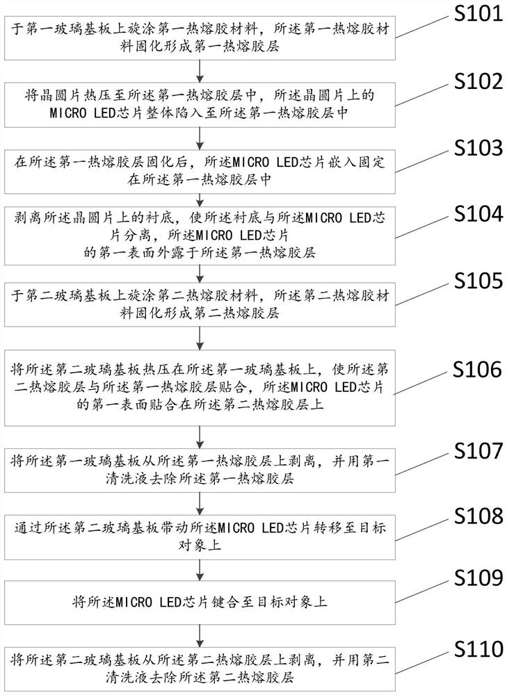
[0043] figure 1 It is a flow chart of the MICRO LED chip transfer method according to the embodiment of the present invention.

[0044] The present invention provides a kind of MICRO LED chip transfer method, comprises the following steps:

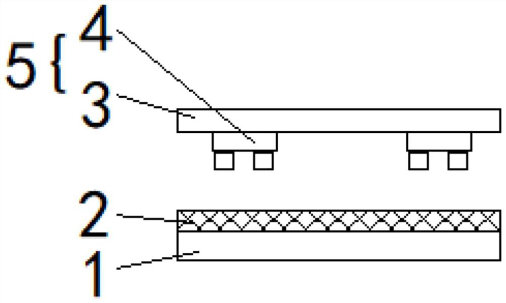
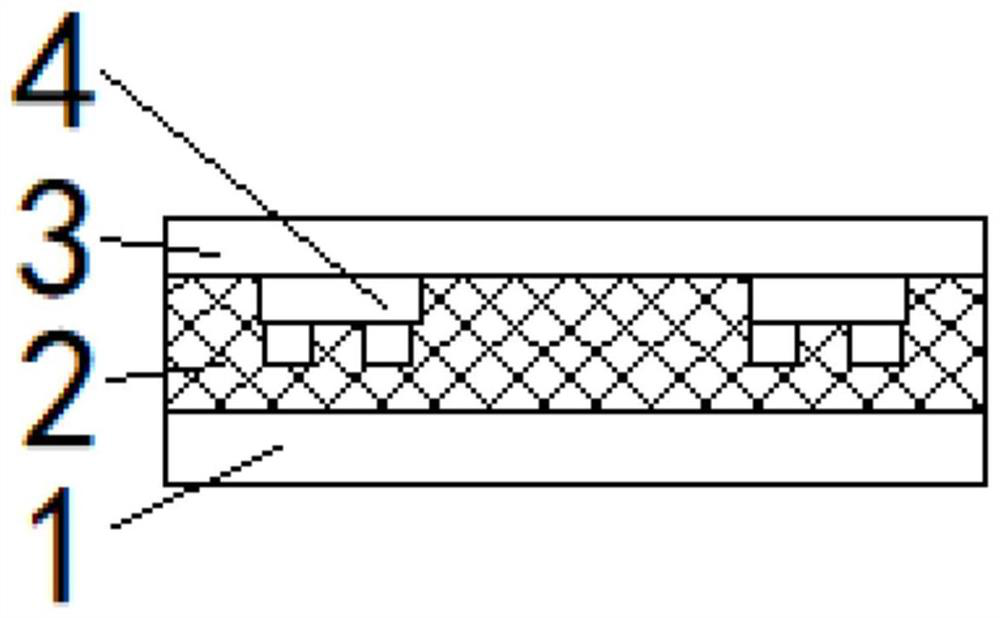
[0045] S101: Spin-coat a first hot-melt adhesive material on the first glass substrate 1, and the first hot-melt adhesive material solidifies to form a first hot-melt adhesive layer 2;

[0046] figure 2 It is a simplified schematic diagram of the principle of step S101 of the MICRO LED chip transfer method according to the embodiment of the present invention. Specifically, the top surface of the first glass substrate 1 is cleaned so that the surface cleanliness of the first glass substrate 1 meets the requirements, and then the surface of the first glass substrate 1 is cleaned. The first hot-melt adhesive material is spin-coated on the top surface of the substrate 1 . After the first hot-melt adhesive material is spin-coated, the desire...

Embodiment 2

[0077] Similar to the implementation of the second transition layer 7, specifically, since the first glass substrate 1 needs to be peeled off from the first hot melt adhesive layer 2 in step S107 of the first embodiment, in order to reduce the first The difficulty of peeling off the glass substrate 1, in the embodiment of the present invention, before the first hot melt adhesive material is spin-coated on the first glass substrate 1, the first transition material is spin-coated on the first glass substrate 1, The first transition material forms a first transition layer, the first hot-melt adhesive material is spin-coated on the first transition layer, and the first transition material is a photosensitive characteristic material;

[0078] Correspondingly, the peeling off the first glass substrate 1 from the first hot melt adhesive layer 2 includes:

[0079] The first transition layer is irradiated by a first light source matched with the first transition material to remove the ...


PUM


Abstract

The invention provides a MICRO LED chip transfer method, which comprises the following steps of: spin-coating a first glass substrate with a first hot melt adhesive material,and curing the first hot melt adhesive material to form a first hot melt adhesive layer; hot-pressing a wafer into the first hot melt adhesive layer; stripping the substrate on the wafer, so that the substrate is separated from the MICRO LED chip; spin-coating a second glass substrate with a second hot melt adhesive material, and curing to form a second hot melt adhesive layer; hot-pressing the second glass substrate on the first glass substrate, so that the second hot melt adhesive layer is attached to the first hot melt adhesive layer; stripping the first glass substrate from the first hot melt adhesive layer, and removing the first hot melt adhesive layer by using a first cleaning solution; enabling the second glass substrate to drive the MICRO LED chip to be transferred to a target object; bonding the MICRO LED chip to the target object; and stripping the second glass substrate from the second hot melt adhesive layer, and removing the second hot melt adhesive layer by using a second cleaning solution. According to the MICRO LED chip transfer method, the chip is better fixed and released by utilizing the polymorphic characteristic that the hot melt adhesive changes along with the temperature.

Description

technical field [0001] The invention relates to the field of chips, in particular to a method for transferring MICRO LED chips. Background technique [0002] At present, MICRO LED chip wafers are facing problems such as difficulty in improving yield rate in LLO (Laser Lift-Off, laser lift-off process) and transfer bonding process. Traditional LLO generally uses UV (Utlraviolet) film and PDMS (Polydimethylsiloxane, polydimethylsiloxane). Although this type of process can improve the LLO yield of the entire wafer, the subsequent trial grab transfer process, due to the thin film Matching problems, such as low chip yield and high probability of electrode drop, cannot carry out the subsequent transfer bonding process well; in the PDMS-LLO process, if the wafers are not bonded properly, it is easy to cause low substrate peeling yield And the chip is easy to be knocked off and other problems, therefore, a suitable transfer process is needed to transfer the MICRO LED chip. Conten...

Claims


Application Information

Patent Timeline
Patent Type & Authority Applications(China)
IPC IPC(8): H01L21/677H01L21/683H01L27/15
CPCH01L21/67781H01L21/6836H01L27/153H01L2221/68386
Inventor 谭孟苹禤劼赵龙黎楚沂李皓
Owner FOSHAN NATIONSTAR OPTOELECTRONICS CO LTD
Learn More