Closed planar three-electrode switch chip based on LTCC process

A switch chip and three-electrode technology, which is applied in the field of closed planar three-electrode switch chips, can solve the problems of high dimensional accuracy and surface finish, unimproved volume, and high manufacturing costs, so as to realize mass production and improve The effect of repeated trigger frequency and reduced production cost

Active Publication Date: 2019-05-24
NANJING UNIV OF SCI & TECH
View PDF3 Cites 3 Cited by
  • Summary
  • Abstract
  • Description
  • Claims
  • Application Information

AI Technical Summary

Problems solved by technology

[0003] However, traditional spark gap switches and vacuum switches are bulky and are assembled with hemispherical electrodes, which are not easy to integrate, and regardless of the overall size, they are basically designed and manufactured based on precision mechanical technology. The requirements for dimensional accuracy and surface finish are quite high, and the assembly precision control needs to be very accurate, so the manufacturing cost is relatively high
Some researchers have also proposed the idea of ​​planar design, but due to the use of traditional mechanical processing, the volume has not been improved, and the low temperature co-fired ceramic technology (Low Temperature Co-fired Ceramic, LTCC), which is characterized by multilayer ceramic components Combined with multi-layer circuit graphics technology, glass / ceramics and other materials are used as the dielectric layer of the circuit, and high-conductivity metals such as Au, Ag, and Cu are used as inner and outer layer electrode materials, and the circuit is printed in parallel printing. Ceramic components or substrates sintered in a sintering furnace about 900°C lower than the melting point of metals

Method used


Image

  • Closed planar three-electrode switch chip based on LTCC process
  • Closed planar three-electrode switch chip based on LTCC process
  • Closed planar three-electrode switch chip based on LTCC process

Examples


Embodiment

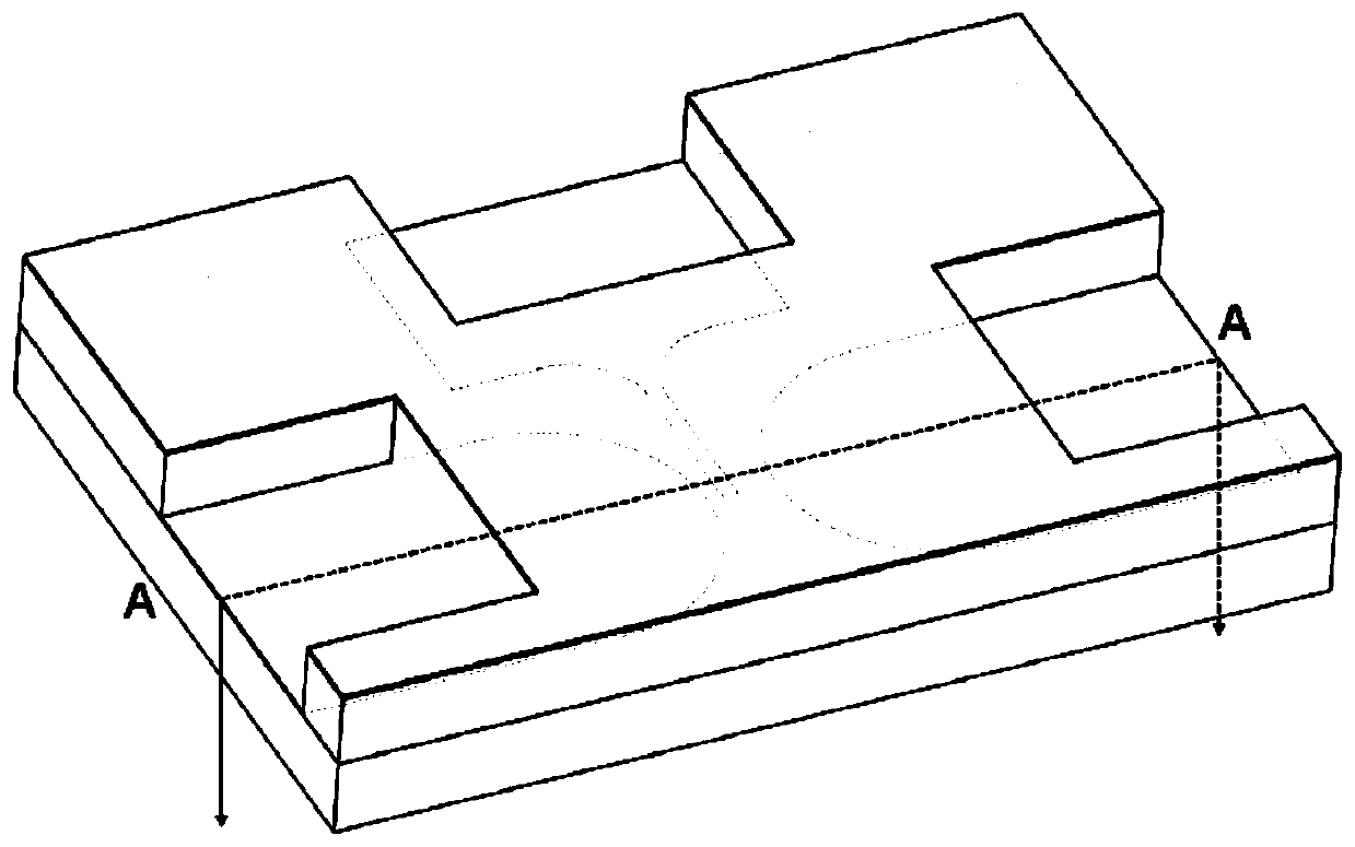
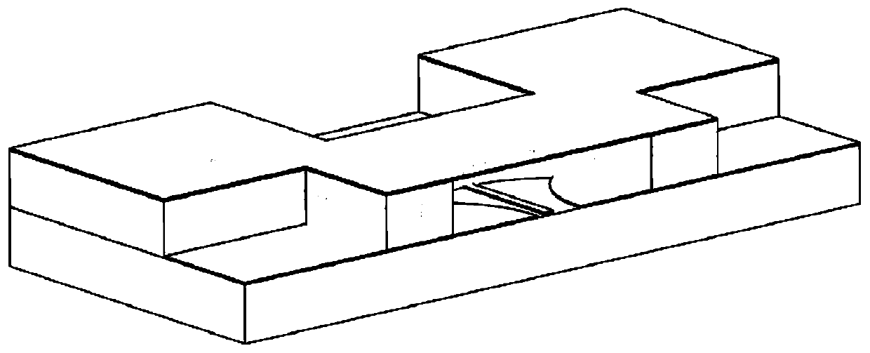
[0053] In this implementation case, a closed planar three-electrode switch chip based on LTCC technology is designed. According to the integrated sintering characteristics of the LTCC process, combined with its processing steps, the switch chip can be divided into four parts: the base layer 1, the metal layer 2, the structure layer A3 and the structure layer B4.

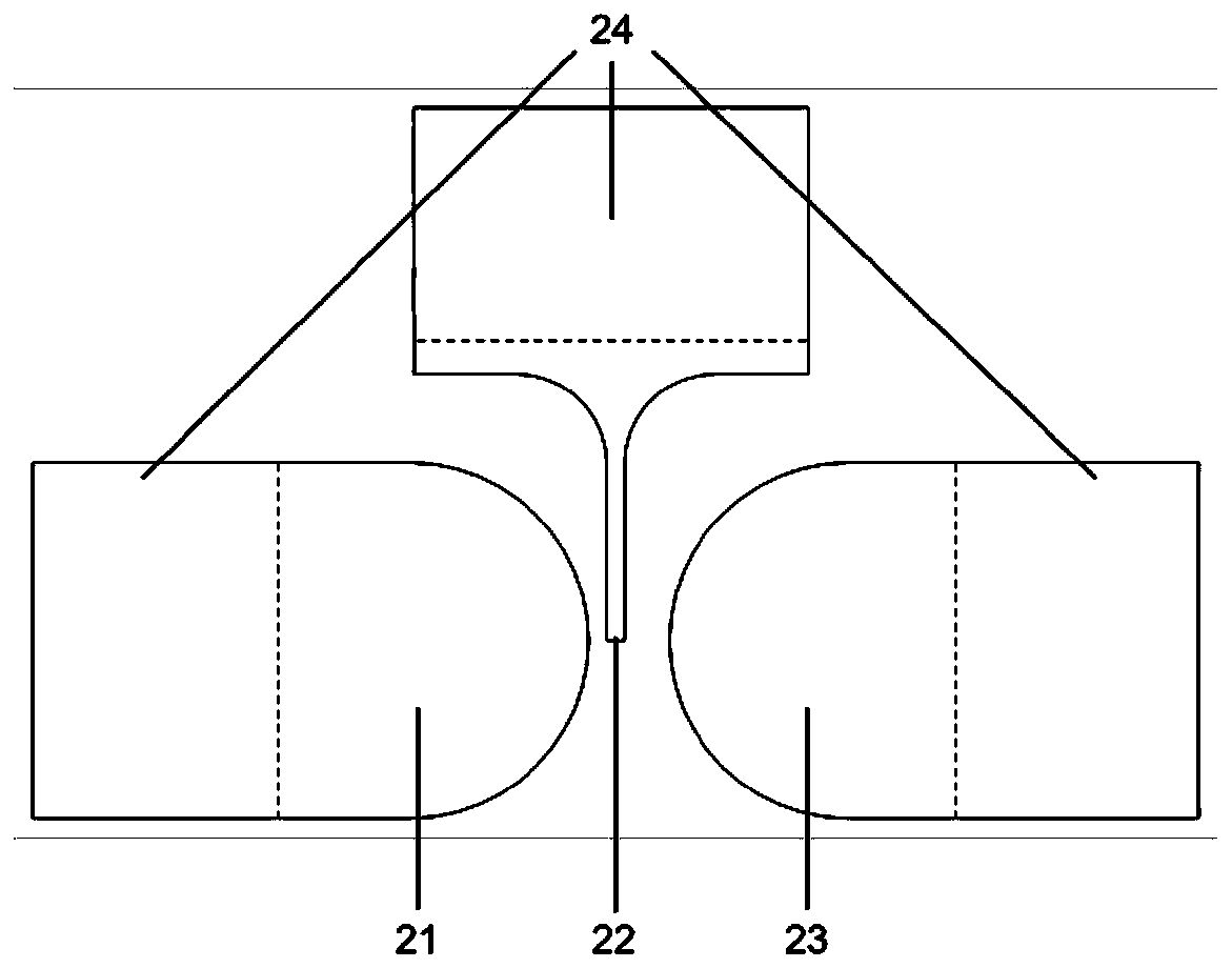
[0054] The base layer 1 is composed of 6-9 layers of green ceramic sheets with a thickness of 110 μm to 114 μm, and serves as a switch carrier in the entire chip. The metal layer 2 adopts the gap screen printing process, uses Au paste as the conductive material, and prints the pattern uniformly on the uppermost green ceramic sheet of the base layer. The thickness of the Au paste is controlled by the thickness of the screen, generally 8 μm to 12 μm; the metal layer 2 may include three electrodes of a planar three-electrode switch, a cathode 21 , a trigger electrode 22 , an anode 23 and a pad 24 for connecting to an ex...


PUM


Abstract

The invention relates to the technical field of high-power pulses and in particular to a closed planar three-electrode switch chip based on an LTCC process. The three electrodes of the switch chip aresealed in a cavity. The switch chip specifically includes a substrate layer which serves as a carrier structure of the planar three-electrode switch chip; a metal layer placed on the substrate layerand including the cathode, the trigger pole and the anode of the switch chip, and bonding pads connected to the cathode, the trigger pole and the anode of the switch; a structural layer A placed overthe metal layer and including an electrode cavity and bonding pad slots exposing the bonding pads; and a structural layer B placed over the structural layer A and including an upper cover of the electrode cavity, and bonding pad slots exposing the bonding pads. The three electrodes of the switch can be sealed in the cavity by using the LTCC process, so that the switch-on capacity of the switch isenhanced and the stability of the switch is improved. Further, the LTCC process can make the switch integrally sintered and manufactured, realize mass production, and improve product consistency and reduces production cost.

Description

technical field [0001] The invention relates to the technical field of high-power pulses, in particular to a closed planar three-electrode switch chip based on LTCC technology. Background technique [0002] Switching technology is the core of high power pulse, which determines the output characteristics of pulse power and plays an important role in many high pulse power application systems. The basic requirements of high-power pulse switches include high withstand voltage, large conduction current, short rise time, small jitter, small inductance and resistance, small electrode burnout, and high repetitive trigger frequency. Due to the instantaneity and reliability of the high-power pulse switch, it is often used as a high-voltage trigger switch in the explosive foil impact initiation circuit. Among them, the vertical hemispherical electrode spark gap switch using the gas discharge breakdown characteristic is the most representative, and has the advantages of relatively simp...

Claims


Application Information

Patent Timeline
Patent Type & Authority Applications(China)
IPC IPC(8): H01T2/02H01T21/00F42B3/10
Inventor 朱朋张秋徐聪杨智覃新汪柯沈瑞琪
Owner NANJING UNIV OF SCI & TECH
Why Eureka
Try Eureka