Chip surface defect detection method based on a convolutional denoising auto-encoder

A self-encoder and surface detection technology, which is applied in the direction of instruments, image data processing, biological neural network models, etc., to achieve the effect of enhancing contrast, high robustness, and suppressing interference

Active Publication Date: 2019-05-31
HEFEI UNIV OF TECH
View PDF10 Cites 21 Cited by
  • Summary
  • Abstract
  • Description
  • Claims
  • Application Information

AI Technical Summary

Problems solved by technology

[0003] In order to overcome the problem of insufficient detection of weak defects in traditional surface defect detection in the prior art, the present invention proposes a chip surface defect detection method based on convolution denoising self-encoder, in order to effectively detect weak defects, so that the chip surface Defects are more easily segmented, which can improve the accuracy of chip surface defect detection

Method used


Image

  • Chip surface defect detection method based on a convolutional denoising auto-encoder
  • Chip surface defect detection method based on a convolutional denoising auto-encoder
  • Chip surface defect detection method based on a convolutional denoising auto-encoder

Examples


Embodiment Construction

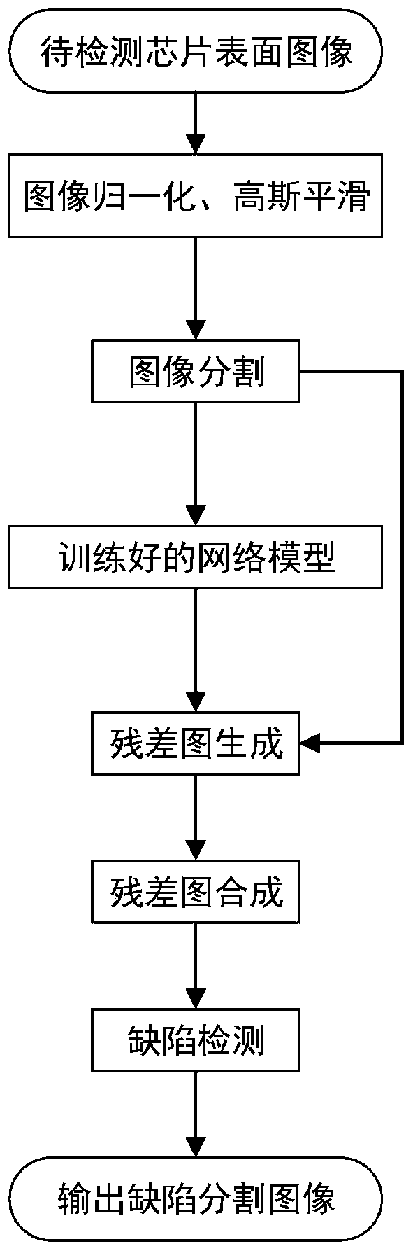
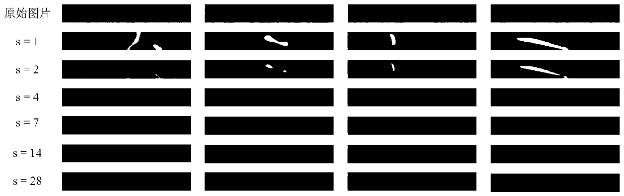
[0040] In this embodiment, a method for detecting chip surface defects based on convolutional denoising autoencoders, such as figure 1 shown, proceed as follows:

[0041] Step 1: Defect-free image reconstruction based on convolutional denoising autoencoder:

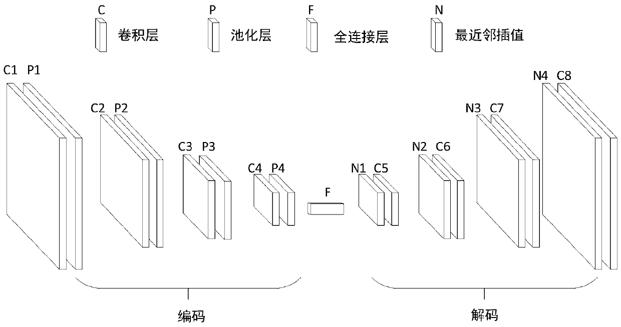
[0042] Step 1.1: Build a convolutional denoising autoencoder as a network model:

[0043]The network model is composed of an encoder, a fully connected layer and a decoder; the encoder is composed of n=4 convolutional layers and 4 pooling layers; the decoder is composed of 4 deconvolution layers; and the encoder and The decoder is connected through a fully connected layer; the 4 deconvolution layers use the nearest neighbor interpolation method and convolution to realize the deconvolution function. like figure 2 As shown, the specific parameters are as follows:

[0044] Input: 28×28×1 single-channel png format picture.

[0045] Encoder: Consists of 4 convolutional (C) layers and 4 pooling (P) layers, each followed b...


PUM


Abstract

The invention discloses a chip surface defect detection method based on a convolutional de-noising auto-encoder. The method comprises the following steps: 1, constructing defect-free image reconstruction based on the convolutional de-noising auto-encoder; 2, constructing a residual image based on the overlapped area; and 3, performing defect detection based on the residual image. According to themethod, weak defects with the characteristics of low defect and background contrast ratio, small defect and the like can be effectively detected, the robustness is very high, and the chip surface detection precision is improved.

Description

technical field [0001] The invention belongs to the technical field of image surface detection, and relates to a chip surface defect detection method based on a convolution denoising self-encoder. Background technique [0002] Chip is a general term for semiconductor component products, which has penetrated into almost all fields such as computing, communication, manufacturing and transportation, and has become an indispensable part of modern society. During the production process, defects such as scratches, scratches, melting, and cracks may appear on the surface of the chip. These defects will affect the appearance and performance of the chip, so they need to be detected and dealt with. Machine vision-based inspection methods are widely used in many aspects of chip production due to their advantages of "low cost and high efficiency", such as identification inspection, pin inspection, wafer inspection and packaging inspection. Chip surface defect detection belongs to the r...

Claims


Application Information

Patent Timeline
Patent Type & Authority Applications(China)
IPC IPC(8): G06T7/00G06T7/11G06N3/04
Inventor 罗月童卞景帅饶永明吴帅张蒙
Owner HEFEI UNIV OF TECH
Why Eureka
Try Eureka