Supercharge Your Innovation With Domain-Expert AI Agents!

A pcb board surface detection method based on contour tolerance algorithm

A PCB board and outline technology, applied in the field of image processing, can solve the problems of the total number of affected areas, the inability to have enough time to accurately intercept the area, and the selection of the size of the intercepted area cannot be accurately grasped, achieving the effect of wide application

Active Publication Date: 2020-09-29
FOSHAN NANHAI GUANGDONG TECH UNIV CNC EQUIP COOP INNOVATION INST +1
View PDF6 Cites 0 Cited by
  • Summary
  • Abstract
  • Description
  • Claims
  • Application Information

AI Technical Summary

Problems solved by technology

First of all, the selection of the size of the intercepted area cannot be accurately grasped in the actual production inspection. In the case of limited inspection time, there is not enough time to accurately intercept the area. When calculating the number of areas, because the gray level of the line edge is gradual, After the binarization threshold, there will be a small area affecting the total number of areas, which will affect the judgment of defects

Method used


Image

  • A pcb board surface detection method based on contour tolerance algorithm
  • A pcb board surface detection method based on contour tolerance algorithm
  • A pcb board surface detection method based on contour tolerance algorithm

Examples


Embodiment

[0033] Embodiment: a method for detecting the surface of a PCB board based on a contour tolerance algorithm.

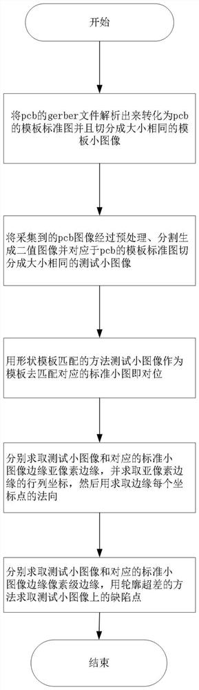
[0034] S1, convert the pcb file into a Gerber file, and then use the GerbMagic software to parse the Gerber file and convert it into a BMP format image; in this way, the binary image of the standard circuit of the pcb bare board is obtained, that is, the standard image, and then cut it into numbers A small image of the same size as a specific size, the segmented standard image is preferentially used to match the object;

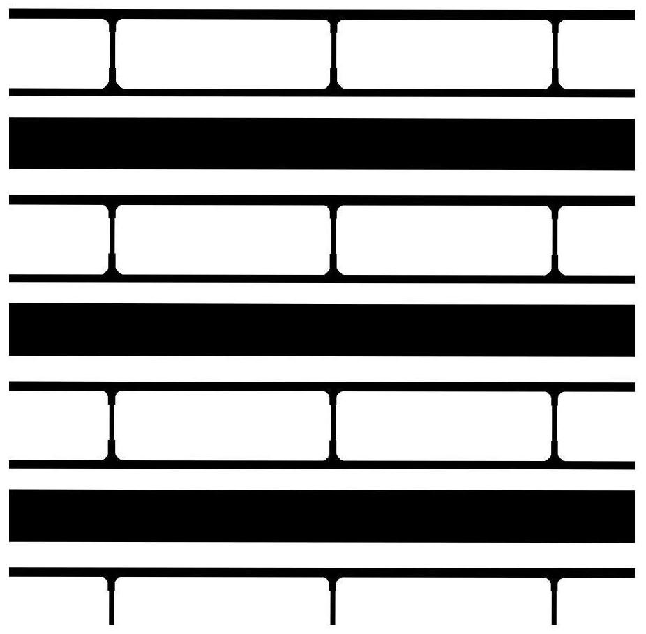
[0035] S2, process the collected image, i.e. denoising, automatic threshold segmentation algorithm to accurately segment the copper surface of the bare board, and then binarize the image, that is, the gray value of the line conductor area is 255, and the gray value of the background area is 0, the binary image is obtained, that is, the test image is divided into several test small images of the same size and specific size, and the divided test small im...


PUM


Abstract

The invention provides a PCB surface detection method based on a contour out-of-tolerance algorithm, and the method comprises the steps: firstly obtaining a PCB bare board template image, then carrying out the processing of the collected image, obtaining a test image, carrying out the template matching of the test image and the template image in place, and finally searching the defects of the testimage through employing the contour out-of-tolerance algorithm. By means of the outline out-of-tolerance method, defects on the PCB can be found in the 360-degree outline direction of the copper surface of the PCB, and limitation of the outline shape is avoided; Almost all PCB defects of open circuit, short circuit, damage, copper surface scratch, copper slag and the like on the PCB can be found;Compared with a traditional method for finding the defects of the PCB by using an image opening and closing operation combined method and other algorithms, the method is more accurate and wider in application range, and almost all defect types on the PCB can be found out. And the defects of missed finding and wrong finding are avoided.

Description

technical field [0001] The invention relates to the field of image processing, in particular to a method for detecting the surface of a PCB board based on a contour tolerance algorithm. Background technique [0002] In the defect detection of PCB board lines based on machine vision, at present, the number and area of ​​connected domains are calculated after intercepting the area to identify short circuit, open circuit, damage, and copper slag defects. This is time-consuming, labor-intensive and low-precision. In the process of image acquisition, other interferences in the planned area caused by factors such as mechanical jitter and lighting, and changes in the number and area of ​​connected domains may easily cause false detection. [0003] At present, most PCB line defects are detected by calculating the number of connected areas in the intercepted area to determine whether the defect is a short circuit or an open circuit, and by comparing the size of the conductor area at ...

Claims


Application Information

Patent Timeline
Patent Type & Authority Patents(China)
IPC IPC(8): G06T7/00G06T7/136
Inventor 张鹏中张璐张美杰胡晓强
Owner FOSHAN NANHAI GUANGDONG TECH UNIV CNC EQUIP COOP INNOVATION INST
Features
  • R&D
  • Intellectual Property
  • Life Sciences
  • Materials
  • Tech Scout
  • Unparalleled Data Quality
  • Higher Quality Content
  • 60% Fewer Hallucinations
Learn More