Film forming apparatus, film forming method and manufacturing method of electronic device

A film-forming device and substrate technology, which is applied in the direction of circuits, electrical components, and electric solid devices, can solve the problems of decreased evaporation accuracy, alignment accuracy, substrate and mask adhesion accuracy, etc.

Active Publication Date: 2019-06-04
CANON TOKKI CORP
View PDF3 Cites 14 Cited by
  • Summary
  • Abstract
  • Description
  • Claims
  • Application Information

AI Technical Summary

Problems solved by technology

However, in this case, as the size of the substrate increases, the central part of the substrate that is not supported by the support portion of the substrate holder and the jig will bend due to the weight of the substrate.
This is the main cause of the decrease in the alignment accuracy of the substrate with respect to the mask and the adhesion accuracy between the substrate and the mask, resulting in a decrease in the accuracy of vapor deposition on the substrate.

Method used


Image

  • Film forming apparatus, film forming method and manufacturing method of electronic device
  • Film forming apparatus, film forming method and manufacturing method of electronic device
  • Film forming apparatus, film forming method and manufacturing method of electronic device

Examples


Embodiment Construction

[0035] Hereinafter, preferred embodiments and examples of the present invention will be described with reference to the drawings. However, the following embodiments and examples are merely illustrative of preferred structures of the present invention, and do not limit the scope of the present invention to these structures. In addition, the hardware structure and software structure, processing flow, manufacturing conditions, dimensions, materials, shapes, etc. of the devices in the following description do not mean that the scope of the present invention is limited to the hardware of the above-mentioned devices unless otherwise specified. Structure and software structure, processing flow, manufacturing conditions, size, material, shape, etc.

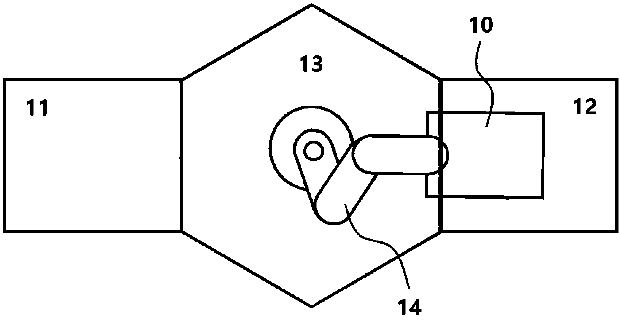
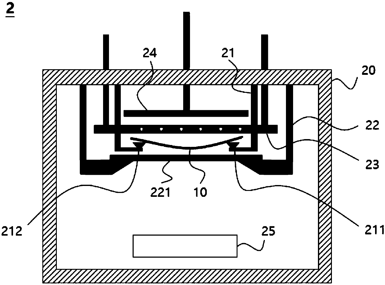
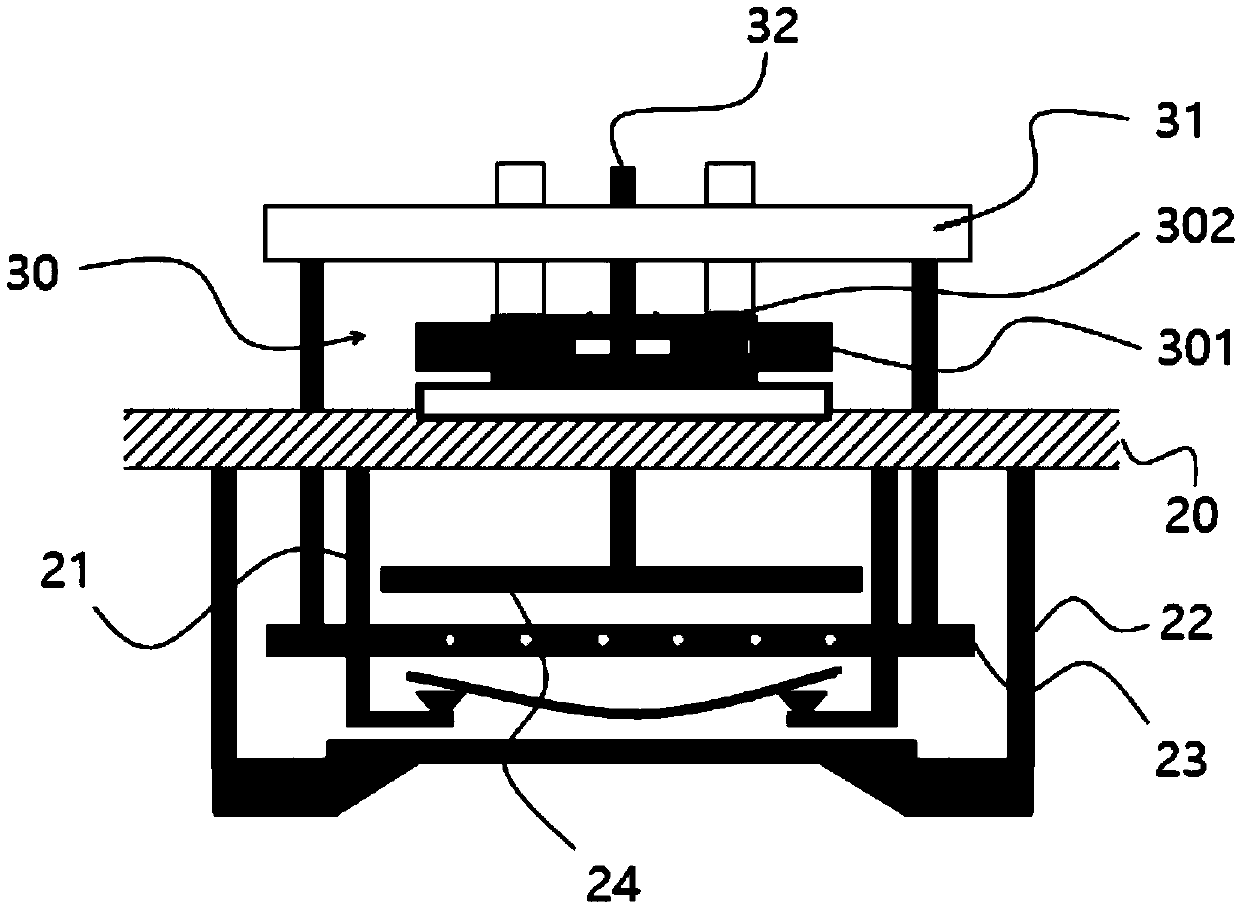
[0036] The present invention can be preferably applied to an apparatus for forming a patterned thin film (material layer) on the surface of a substrate by vacuum evaporation. As the material of the substrate, any material such as glass, ...


PUM


Abstract

The invention provides a film forming apparatus, a film forming method, and an electronic device manufacturing method. The film forming apparatus according to the present invention is used for forminga vapor deposition material on a substrate via a mask, and includes: a vacuum chamber defining a space in which a vapor deposition process is performed; the substrate adsorption mechanism is arrangedin the vacuum chamber and is used for adsorbing a substrate; the magnetic force applying mechanism is arranged above the substrate adsorbing mechanism in the vacuum chamber and is used for applying magnetic force to the mask; and an alignment station, the alignment table is arranged on the first outer surface of the vacuum chamber; and a rotation mechanism for moving or rotating the substrate suction mechanism and the magnetic force application mechanism in at least one of a first direction, a second direction intersecting with the first direction, and a rotation direction with a third direction intersecting with the first direction and the second direction as an axis.

Description

technical field [0001] The present invention relates to a film forming apparatus and a film forming method, and more particularly to a film forming apparatus having a structure in which an elevating mechanism of a substrate suction mechanism and an elevating mechanism of a magnetic force applying mechanism are mounted on an alignment table, and a film forming method using the film forming apparatus . Background technique [0002] Recently, an organic EL display device has attracted attention as a flat panel display device. Organic EL display devices are self-luminous displays, and their characteristics such as response speed, viewing angle, and thinness are superior to liquid crystal panel displays. Existing LCD panel displays. In addition, the field of application thereof is expanding in automotive displays and the like. [0003] The element of the organic EL display device has a basic structure in which an organic substance layer that emits light is formed between two o...

Claims


Application Information

Patent Timeline
Patent Type & Authority Applications(China)
IPC IPC(8): C23C14/04C23C14/24C23C14/50
CPCC23C14/042C23C14/24C23C14/50C23C14/52C23C14/54H10K71/164H10K71/166
Inventor 石井博柏仓一史
Owner CANON TOKKI CORP
Why Eureka
Try Eureka