Processing technology of SOC chip IP clock in DFT
A chip and clock technology, applied in the processing field of SOC chip IP clock in DFT, can solve the problems of unmeasurable timingpath of OCC circuit, failure of chip scan chain test, large chip port requirements, etc., to achieve improved test coverage, Improve test coverage and reduce requirements
- Summary
- Abstract
- Description
- Claims
- Application Information
AI Technical Summary
Problems solved by technology
Method used
Image

Examples
Embodiment 1
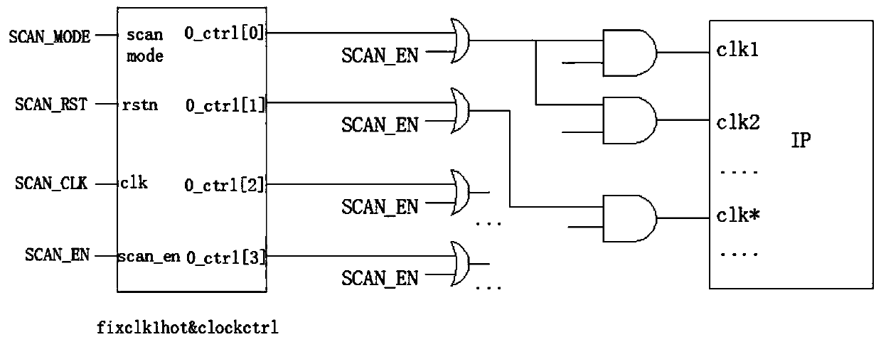
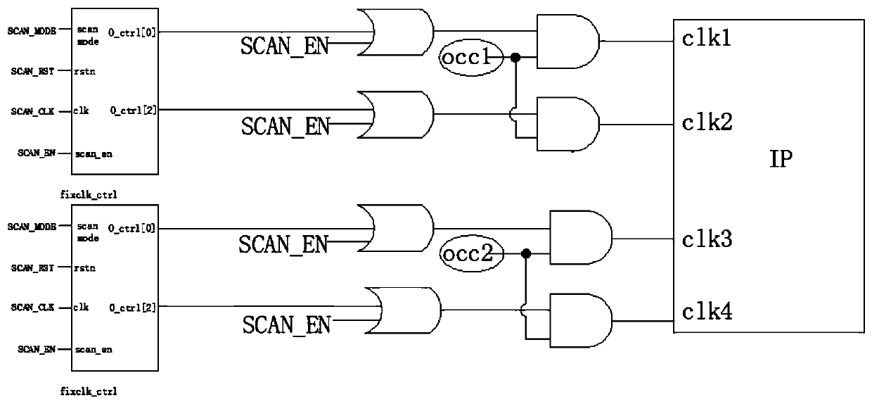
[0025] A kind of processing technology of SOC chip IP clock in DFT, the concrete steps of processing technology are:
[0026] (1) Perform DFT scan chain test on IP clock;
[0027] (2) Introduce the clock control circuit into the DFT scan chain test circuit, and output multi-bit control signals;
[0028] (3) introduce this signal to the corresponding IP clock;
[0029] (4) Place the SOC chip on the ATE base, so that the probe on the ATE base is in contact with the SOC chip;
[0030] (5) After the ATPG tool generates specific test vectors, test the SOC chip on the ATE base station according to the test vectors.
[0031] The clock control circuit is added to the scan circuit of the entire SOC chip together with the scan chain, so that each control signal can be flexibly turned on when the ATPG generates test vectors.
[0032] The clock circuit is a control circuit that does not reverse simultaneously in the capture mode during the DFT scan chain test.
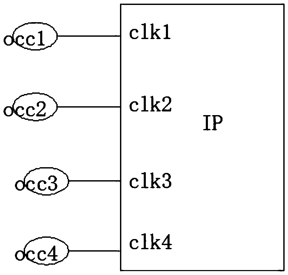
[0033] Such as figure...
PUM
 Abstract
Description
Claims
Application Information