

Conductive pattern, display device including the same, and method of manufacturing conductive pattern
一种导电图案、显示设备的技术,应用在半导体/固态器件制造、电路、电气元件等方向,能够解决难以确保工艺可靠性、信号布线损坏等问题,达到改善显示质量、信号延迟降低、防止膜不均匀的效果
- Summary
- Abstract
- Description
- Claims
- Application Information
AI Technical Summary
Problems solved by technology
Method used
Image

Examples
Embodiment Construction
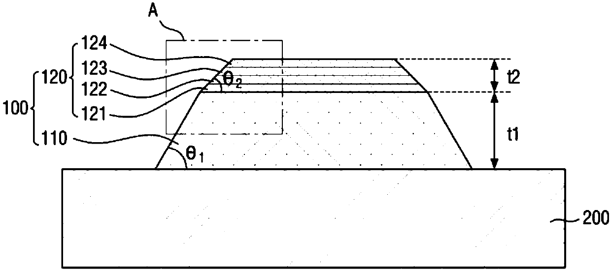
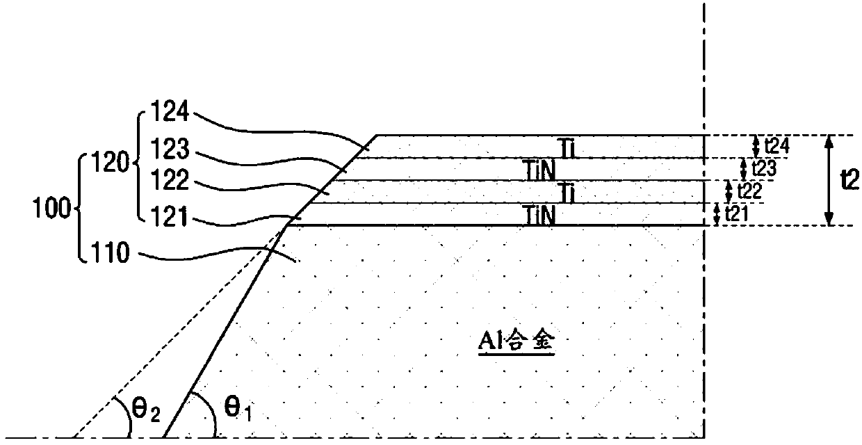
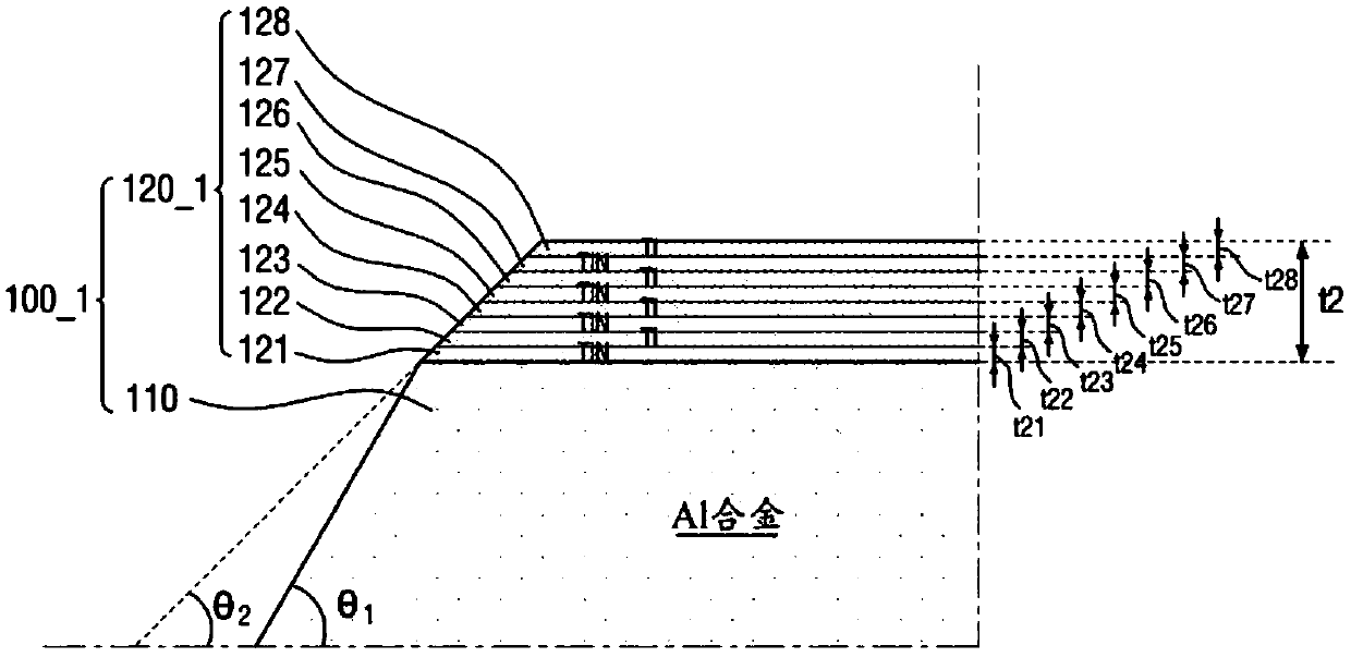
[0046]In the following description, for purposes of explanation, numerous specific details are set forth in order to provide a thorough understanding of various exemplary embodiments or implementations of the invention. As used herein, "embodiment" and "implementation" are interchangeable words as non-limiting examples of devices or methods disclosed herein that employ one or more of the inventive concepts. It is to be understood, however, that the various exemplary embodiments may be practiced without these specific details or with one or more equivalent arrangements. In other instances, well-known structures and devices are shown in block diagram form in order to avoid unnecessarily obscuring the various exemplary embodiments. Additionally, the various exemplary embodiments may differ, but are not necessarily exclusive. For example, specific shapes, configurations, and characteristics of an exemplary embodiment may be used or implemented in another exemplary embodiment with...
PUM
| Property | Measurement | Unit |
|---|---|---|
| angle | aaaaa | aaaaa |
| angle | aaaaa | aaaaa |
Abstract
Description
Claims
Application Information