Device testing system and method
A test system and device technology, applied in the field of silicon carbide device test platform, can solve problems such as difficult to test the performance of switching devices, single drive signal, insufficient switching frequency, etc., and achieve the effect of high engineering application value
- Summary
- Abstract
- Description
- Claims
- Application Information
AI Technical Summary
Problems solved by technology
Method used
Image

Examples
Embodiment Construction
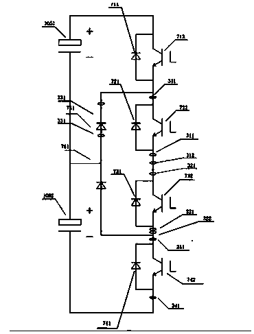
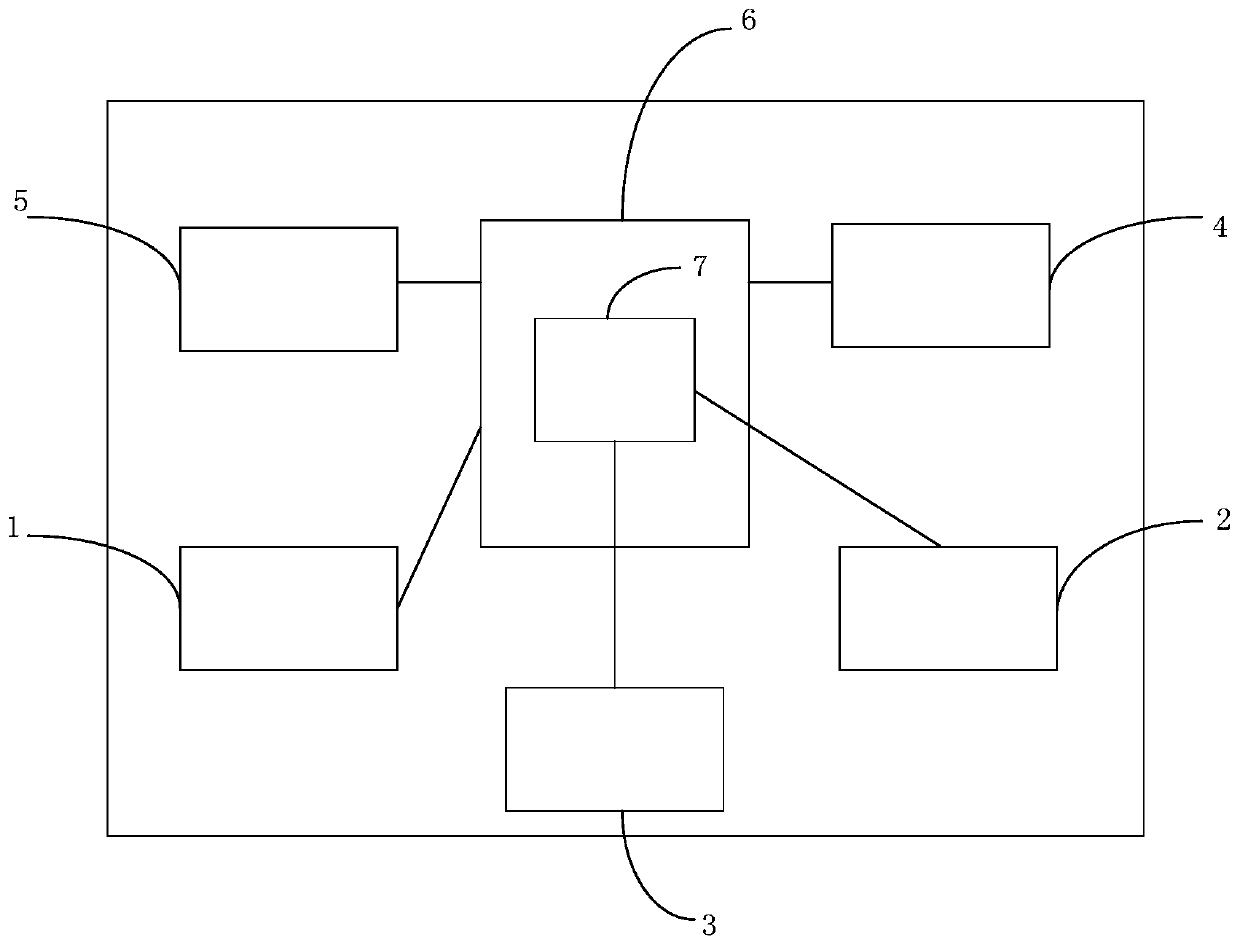
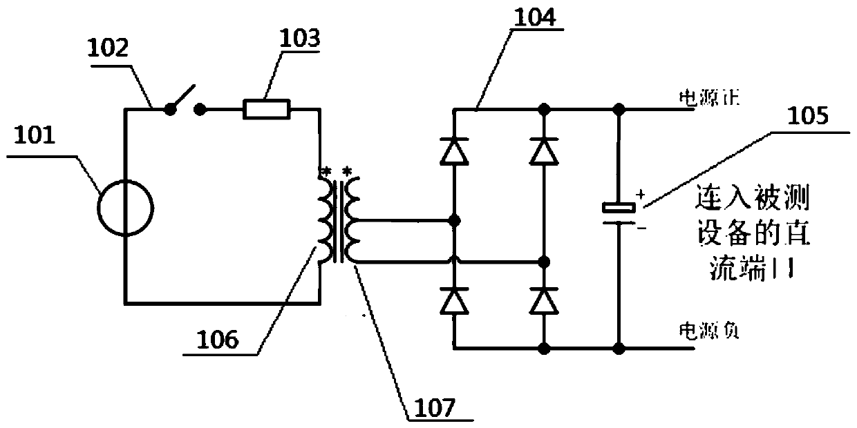
[0057] In order to make the purpose, technical solutions and advantages of the embodiments of the present invention clearer, the technical solutions in the embodiments of the present invention will be clearly and completely described below in conjunction with the drawings in the embodiments of the present invention. Obviously, the described embodiments are only It is a part of embodiments of the present invention, but not all embodiments. The components of the embodiments of the invention generally described and illustrated in the figures herein may be arranged and designed in a variety of different configurations. Accordingly, the following detailed description of the embodiments of the invention provided in the accompanying drawings is not intended to limit the scope of the claimed invention, but merely represents selected embodiments of the invention. Based on the embodiments of the present invention, all other embodiments obtained by those skilled in the art without making...
PUM
 Abstract
Description
Claims
Application Information
PatSnap Eureka turns technology decisions into work you can execute. Powered by our Innovation Knowledge Graph, it runs expert workflows across engineering, life sciences, materials and intellectual property. Get your review-ready output in minutes.


