
OLED display panel and a method for manufacturing same, and OLED display device

A technology for display panels and display areas, applied in semiconductor/solid-state device manufacturing, semiconductor devices, electrical components, etc., can solve the problems of large edge climbing distance, difficult to control the fluidity of the second packaging layer, poor thickness uniformity, etc. The effect of reducing the climbing distance, avoiding poor mura, and improving the uniformity of edge thickness

Pending Publication Date: 2019-06-07
BOE TECH GRP CO LTD +1
View PDF0 Cites 30 Cited by
  • Summary
  • Abstract
  • Description
  • Claims
  • Application Information

AI Technical Summary

Problems solved by technology

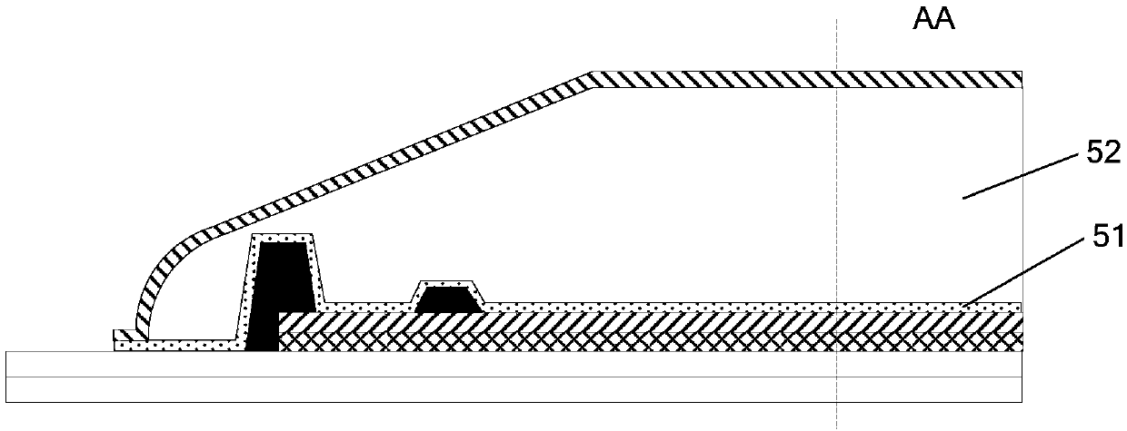
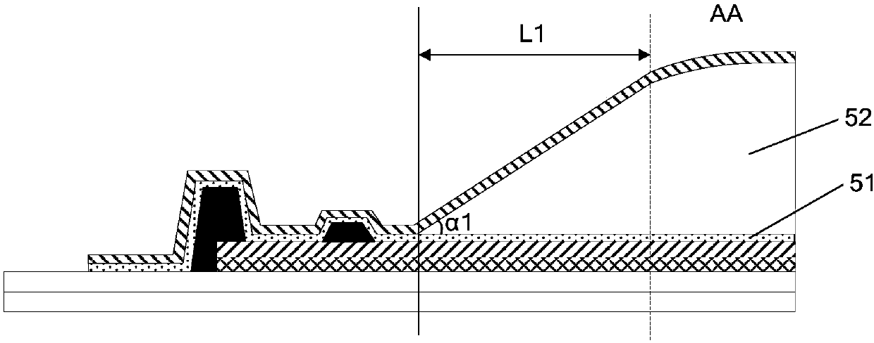
[0005] Aiming at the above-mentioned deficiencies in the prior art, the present invention provides an OLED display panel, a manufacturing method thereof, and an OLED display device to at least partly solve the problems of the OLED display panel. In the encapsulation process, the fluidity of the organic second encapsulation layer is difficult to control, the edge climbing distance is large and the thickness uniformity is poor

Method used


Image

  • OLED display panel and a method for manufacturing same, and OLED display device
  • OLED display panel and a method for manufacturing same, and OLED display device
  • OLED display panel and a method for manufacturing same, and OLED display device

Examples


Embodiment Construction

[0038] The technical solutions in the present invention will be clearly and completely described below in conjunction with the accompanying drawings in the present invention. Apparently, the described embodiments are part of the embodiments of the present invention, not all of them. Based on the embodiments of the present invention, all other embodiments obtained by persons of ordinary skill in the art without making creative efforts belong to the protection scope of the present invention.

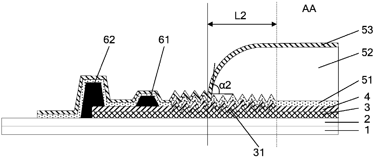
[0039] combine as figure 2 As shown, the present invention provides an OLED display panel, which includes: a base substrate 1, a back plate (Back Plate, BP) 2 and a planarization layer (PVD) 3 formed on the base substrate 1 in sequence , the organic light-emitting functional layer 4 , the first encapsulation layer 51 and the second encapsulation layer 52 . The organic light emitting functional layer 4 may include: an anode, a hole injection layer, a hole transport layer, a light emitting...


PUM


Abstract

The present invention provides an OLED display panel and a method for manufacturing the same, and an OLED display device. A concave-convex structure is arranged at one side, far away from a substrate,on a planarization layer, after an organic light-emitting functional layer and an inorganic first package layer are formed on the planarization layer, positions of the organic light-emitting functional layer and the first package layer corresponding to the concave-convex structure are non-flat surfaces, namely concave-convex structures with the same shapes are formed at the positions, corresponding to the concave-convex structure, on the organic light-emitting functional layer and the first package layer; when an organic second package layer is formed, the non-flat surface of the first package layer can block the flow of the second package layer to a certain extent to reduce the liquidity of the second package layer, reduce the climbing distance of the edge of the second package layer andincrease the edge stress and an angle of gradient so as to achieve the product narrow-frame design, improve the thickness uniformity of the edges of the second package layer, avoid bad mura of a non-display area and ensure the package effect.

Description

technical field [0001] The invention relates to the field of display technology, in particular to an OLED display panel, a preparation method thereof, and an OLED display device. Background technique [0002] OLED (Organic Light-Emitting Diode, Organic Light-Emitting Diode) devices have become a very Competitiveness and prospects for next-generation display technologies. The organic light-emitting materials and cathode materials used in OLED devices are particularly sensitive to water and oxygen. Too much humidity or too high oxygen content will affect the service life of OLED devices. In order to effectively block the influence of water and oxygen on the OLED device, it needs to be encapsulated. [0003] TFE (Thin Film Encapsulation Technology) packaging has excellent water and oxygen barrier effects, and can be used for flexible packaging. It has become the mainstream packaging technology for flexible OLED display panel packaging. However, in the TFE encapsulation proce...

Claims


Application Information

Patent Timeline
Patent Type & Authority Applications(China)
IPC IPC(8): H01L51/52H01L51/56
CPCH10K71/00H10K59/873H10K50/8426H10K50/844
Inventor 王格蒋志亮王婷乔梓
Owner BOE TECH GRP CO LTD
Learn More