A kind of preparation method of chip

A chip and chip area technology, applied in semiconductor/solid-state device manufacturing, electrical components, circuits, etc., can solve the problem of chip volume increase, achieve the effect of reducing chip volume, ensuring effective connection, and reducing damage

Active Publication Date: 2021-07-27
SHANGHAI NATLINEAR ELECTRONICS CO LTD
View PDF5 Cites 0 Cited by
  • Summary
  • Abstract
  • Description
  • Claims
  • Application Information

AI Technical Summary

Problems solved by technology

[0002] The semiconductor wafer includes a chip area and a scribe groove area, and the existing test pads are located in the chip area, which increases the chip volume

Method used


Image

  • A kind of preparation method of chip
  • A kind of preparation method of chip
  • A kind of preparation method of chip

Examples


Embodiment Construction

[0045] Embodiments of the present invention are described below through specific examples, and those skilled in the art can easily understand other advantages and effects of the present invention from the content disclosed in this specification. The present invention can also be implemented or applied through other different specific implementation modes, and various modifications or changes can be made to the details in this specification based on different viewpoints and applications without departing from the spirit of the present invention.

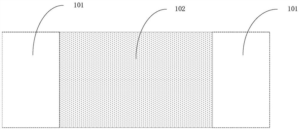
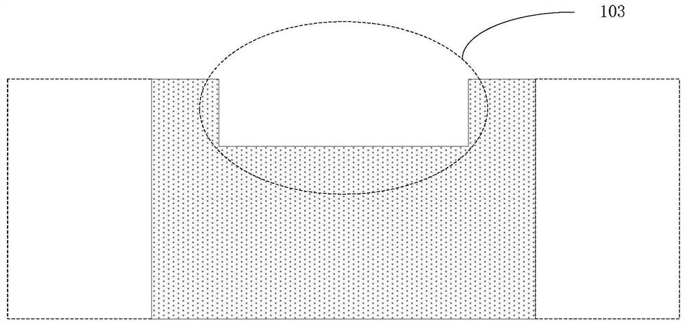
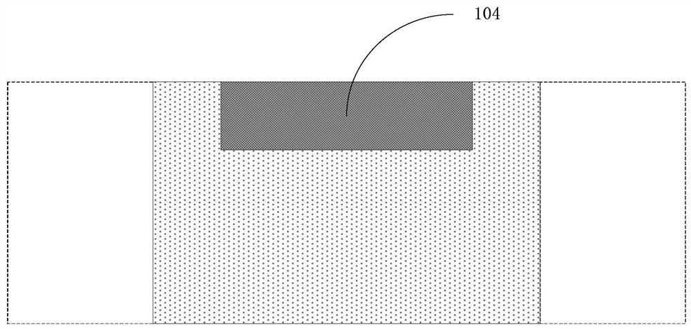
[0046] see Figure 1 to Figure 11 . It should be noted that the diagrams provided in this embodiment are only schematically illustrating the basic idea of ​​the present invention, and only the components related to the present invention are shown in the diagrams rather than the number, shape and shape of the components in actual implementation. Dimensional drawing, the type, quantity and proportion of each component can be changed ar...


PUM


Abstract

The present invention provides a method for preparing a chip, comprising the steps of: providing a semiconductor wafer, the semiconductor wafer includes a plurality of chip regions and scribe regions between the chip regions; A test pad structure, the test pad structure includes a test pad groove formed in the scribe groove area and a test pad conductive layer formed in the test pad groove, the test pad structure Electrically connected to the chip area; using a laser to form a scribe groove in the scribe groove area to remove the conductive layer of the test pad in the scribe groove; based on the scribe groove to the Semiconductor wafers are diced. The chip preparation method of the present invention can reduce the difficulty of scribing, improve the efficiency of slicing, protect the scribing knife, reduce the damage to the internal chip during slicing, reduce the volume of the chip, and improve the integration of the chip. The process is simple and can Mass production.

Description

technical field [0001] The invention belongs to the field of semiconductor manufacturing, in particular to a method for preparing a chip. Background technique [0002] A semiconductor wafer includes a chip area and a scribe groove area, and existing test pads are located in the chip area, which increases the volume of the chip. Conventionally, after functional testing, the monolithic IC must be separated from the substrate, using a dicing knife or scribe lift-off technique to separate the wafer into individual chips. This method requires the wafer to be precisely positioned on a precision workbench, and then scribed according to pattern rules in the X and Y directions with a diamond scribe or a diamond scribe. The scribe or scribe makes a shallow mark on the surface of the wafer, which actually breaks the crystal orientation of the wafer. Then remove the scribed wafer from the workbench, put it upside down on a flexible support pad, and apply pressure to it with a cylindri...

Claims


Application Information

Patent Timeline
Patent Type & Authority Patents(China)
IPC IPC(8): H01L21/78
Inventor 刘桂芝周尧崔凤敏蒋小强
Owner SHANGHAI NATLINEAR ELECTRONICS CO LTD
Why Eureka
Try Eureka