Method for measuring the surface shape of doped silicon wafer based on near-infrared low-coherent light

A technology of surface topography measurement and low-coherence light, which is applied in the direction of measuring devices, optical devices, instruments, etc., can solve the problems of surface measurement after doping silicon wafers, and improve the contrast of interference fringes, improve efficiency and accuracy , the effect of increasing the range

Inactive Publication Date: 2019-06-21
HEFEI UNIV OF TECH
View PDF5 Cites 1 Cited by
  • Summary
  • Abstract
  • Description
  • Claims
  • Application Information

AI Technical Summary

Problems solved by technology

However, this method still cannot solve the problem

Method used


Image

  • Method for measuring the surface shape of doped silicon wafer based on near-infrared low-coherent light
  • Method for measuring the surface shape of doped silicon wafer based on near-infrared low-coherent light
  • Method for measuring the surface shape of doped silicon wafer based on near-infrared low-coherent light

Examples


Example Embodiment

[0020] The technical solutions in the embodiments of the present invention will be clearly and completely described below in conjunction with the accompanying drawings.

[0021] A method for measuring the surface topography of a silicon wafer doped with near-infrared low-coherence light, comprising the following steps:

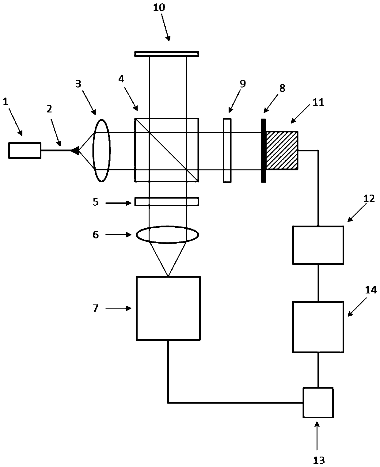
[0022] 1) The measurement device of a near-infrared broadband light source is selected; a near-infrared light source with a center wavelength of 1550nm and a bandwidth of 50nm is selected.

[0023] 2) Build a Michelson interferometer with a movable reference arm and a measuring arm. The circuit board of the Michelson interferometer controls the stepping motor, so that the optical path difference between the reference optical path and the measured optical path is gradually changed, and the silicon wafer Scanning interference of the surface to be measured;

[0024] 3) Finally, the near-infrared camera is used to continuously photograph the interferogram, and the interfe...


PUM


Abstract

The invention belongs to the field of silicon wafer measurement and discloses a method for measuring the surface shape of a doped silicon wafer based on near-infrared low-coherent light. The method ischaracterized by comprising the following steps of 1) selecting a measuring device for a near-infrared broadband light source; 2) constructing a Michelson interferometer having a movable reference arm and a measuring arm, using the Michelson interferometer's circuit board to control a stepping motor in order that an optical path difference between the reference arm and the measuring arm is gradually changed to realize scanning interference on the to-be-measured surface of the silicon wafer; and 3) finally, continuously capturing an interferogram by using a near-infrared camera and demodulating interference information by an algorithm to obtain the physical properties of the doped silicon wafer to be measured. The method improves the contrast of the silicon wafer measurement accuracy andinterference fringes and the efficiency and accuracy of surface shape reconstruction.

Description

Technical field [0001] The invention belongs to the field of silicon wafer measurement, and particularly relates to a method for measuring the surface topography of a silicon wafer doped with near-infrared low-coherence light. Background technique [0002] Silicon wafers are widely used as substrates in semiconductor production. Currently, semiconductors are moving toward larger sizes and thinner thicknesses. The large size can increase the output of semiconductor production, and the thinner silicon wafers are conducive to the 3D packaging of semiconductors. The silicon wafers can be stacked in a certain area to obtain higher performance. In the photolithography process, light is transmitted through the pattern on the mask and projected onto the surface of the silicon wafer through the optical imaging system. If the change in the geometric thickness of the silicon wafer is greater than the focal depth of the imaging system, the manufactured pattern may be deformed or even usele...

Claims


Application Information

Patent Timeline
IPC IPC(8): G01B11/30
Inventor 于连栋闫新宇程杰卞点陆洋
Owner HEFEI UNIV OF TECH
Why Eureka
Try Eureka