Fabrication method of array substrate, array substrate and display device

A technology of an array substrate and a manufacturing method, applied in the field of array substrates and display devices, can solve the problems of poor display effect, easy occurrence of dislocation and disconnection, etc., and achieve the effect of ensuring display effect, avoiding disconnection and avoiding dislocation

Active Publication Date: 2019-06-21
BOE TECH GRP CO LTD +1
View PDF5 Cites 4 Cited by
  • Summary
  • Abstract
  • Description
  • Claims
  • Application Information

AI Technical Summary

Problems solved by technology

[0004] Embodiments of the present invention provide a method for manufacturing an array substrate, an array substrate, and a display device, so as to solve the problem of misalignment and disconnection easily occurring in the electrical connection of the front and back of the Micro-LED display panel used for splicing in the prior art, resulting in Problems with poor display

Method used


Image

  • Fabrication method of array substrate, array substrate and display device
  • Fabrication method of array substrate, array substrate and display device
  • Fabrication method of array substrate, array substrate and display device

Examples


Embodiment Construction

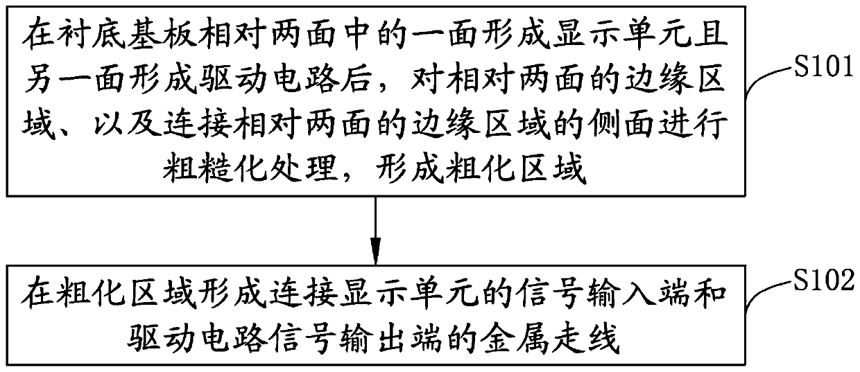
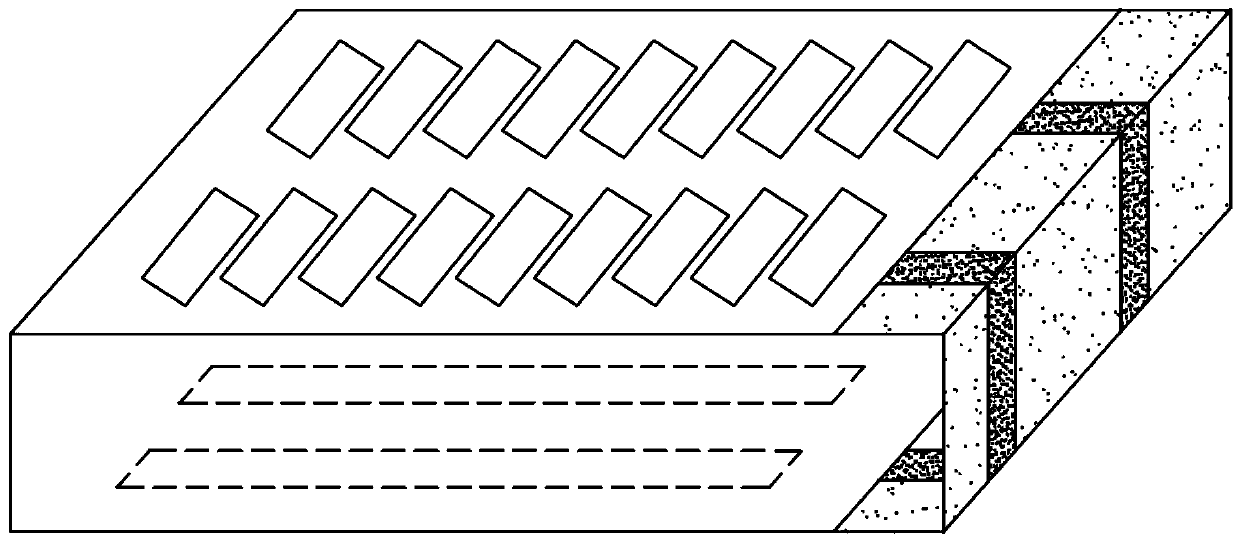
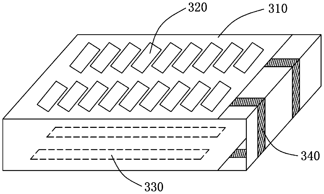
[0030] The following will clearly and completely describe the technical solutions in the embodiments of the present invention with reference to the accompanying drawings in the embodiments of the present invention. Obviously, the described embodiments are some of the embodiments of the present invention, but not all of them. Based on the embodiments of the present invention, all other embodiments obtained by persons of ordinary skill in the art without creative efforts fall within the protection scope of the present invention.

[0031] Micro LED is a new generation of display technology, which has higher brightness, better luminous efficiency and lower power consumption than the existing Organic Light-Emitting Diode (OLED) technology, so Micro LED display devices are becoming more and more popular . Sometimes in order to realize the large-size display of the Micro-LED display device, it is necessary to splice together multiple small-sized Micro-LED display panels, wherein the ...


PUM


Abstract

The invention provides a fabrication method of an array substrate, the array substrate and a display device. The fabrication method of the array substrate comprises the steps of forming a display uniton one of two opposite surfaces of a substrate, forming a driving circuit on the other surface, and roughing edge regions of the two opposite surfaces and side surfaces connected with the edge regions of the two opposite surfaces to form a rough region; and forming a signal input end connected with the display unit and a metal wire of a signal output end of the driving circuit at the rough region. With the fabrication method of the array substrate, the array substrate and the display device, provided by the invention, the display effect of the display device can be ensured.

Description

technical field [0001] The present invention relates to the field of display technology, in particular to a manufacturing method of an array substrate, an array substrate and a display device. Background technique [0002] The Micro-LED display panel has the advantages of ultra-high pixel count, ultra-high resolution, low energy consumption, and long life. Compared with Organic Light-Emitting Diode (OLED), it can The distance is reduced to um to further optimize the display effect, so Micro-LED display devices are becoming more and more popular in the market. [0003] At present, in order to realize the large-size display of the Micro-LED display device, it is necessary to splice multiple small-sized Micro-LED display panels together, wherein the front and back sides of each Micro-LED display panel need to be electrically connected. In the prior art, the way of realizing the electrical connection between the front and the back of the Micro-LED display panel is prone to disl...

Claims


Application Information

Patent Timeline
Patent Type & Authority Applications(China)
IPC IPC(8): H01L21/84H01L27/12H01L27/15
CPCH01L25/167G09G3/32H01L25/0753H01L27/124H01L27/1259
Inventor 齐永莲刘超曲连杰赵合彬张珊贾宁石广东刘帅
Owner BOE TECH GRP CO LTD
Why Eureka
Try Eureka