Electronic equipment shell, preparation method thereof and electronic equipment

A technology for electronic equipment and shells, which is applied in the field of electronic equipment shells and their preparation, and can solve the problems of limited appearance effects of electronic equipment shells, inability to effectively adjust brightness and optical effects, and needs to be improved.

CN109927471AInactive Publication Date: 2019-06-25GUANGDONG OPPO MOBILE TELECOMM CORP LTD
5 Cites 29 Cited by

Patent Information

Authority / Receiving Office
CN · China
Patent Type
Applications(China)
Current Assignee / Owner
Publication Date
2019-06-25
Estimated Expiration
Not applicable · inactive patent

Smart Images

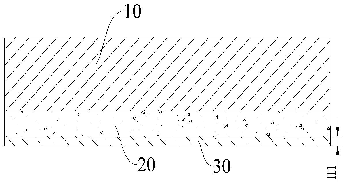
  • Figure 1
    Figure 1
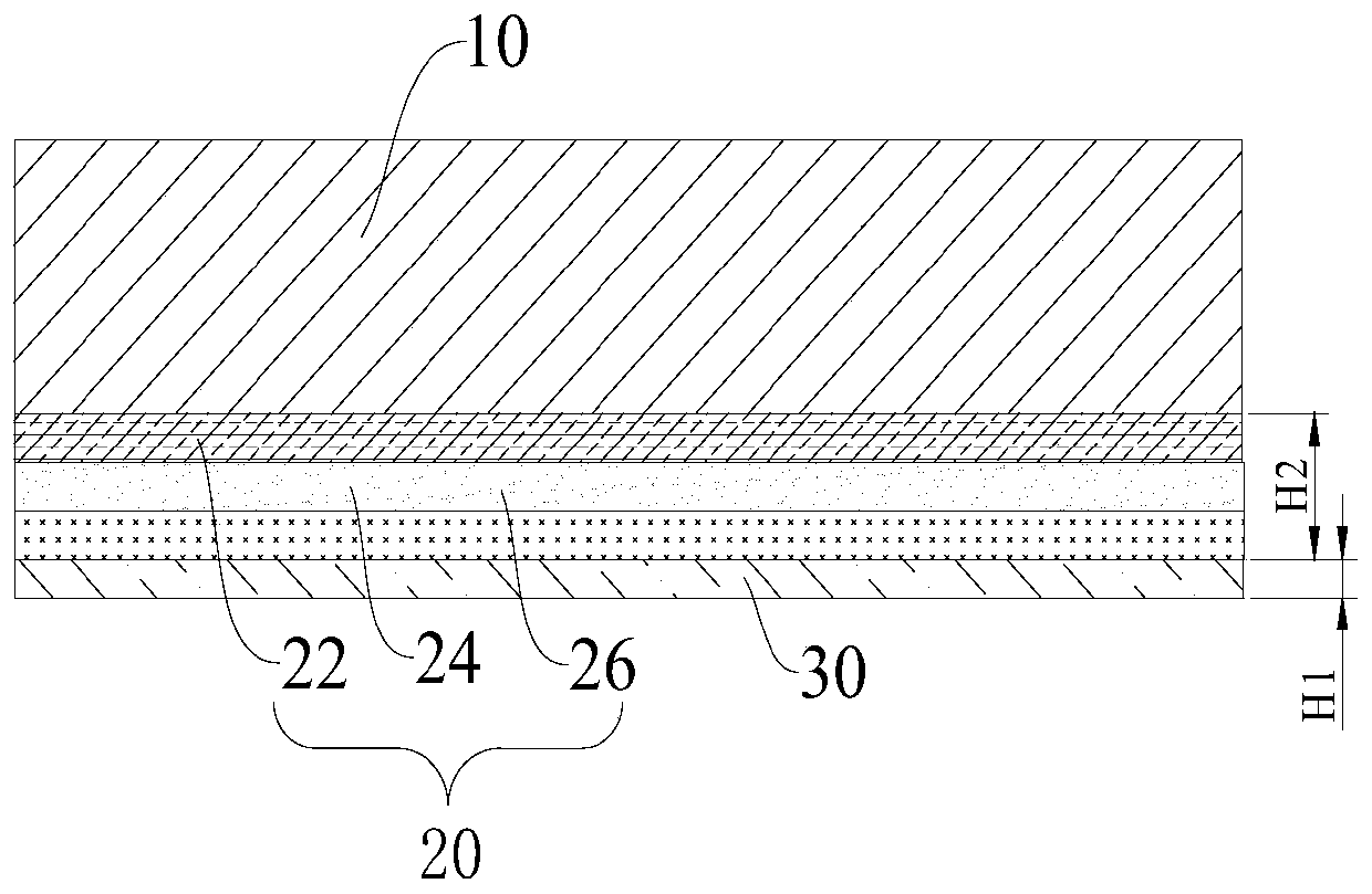
  • Figure 2
    Figure 2
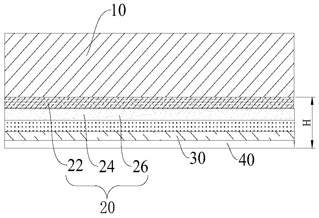
  • Figure 3
    Figure 3
Patent Text Reader

Abstract

The invention provides an electronic equipment shell, a preparation method thereof and electronic equipment. The electronic equipment shell comprises a base material, an optical coating layer and a metal functional layer, wherein the optical coating layer is arranged on one side of the base material; and the metal functional layer is arranged on the surface, away from the base material, of the optical coating layer, and the metal functional layer is made of indium, tin or indium tin alloy. The metal functional layer and the metal functional layer of the electronic equipment shell can cooperateand achieve the synergistic effect, a plurality of optical effect different in color and brightness are realized, accordingly, the more diversified, bright and colorful appearance effect is achieved,the increasingly higher aesthetic requirements of users are met, and the better user experience is provided.
Need to check novelty before this filing date? Find Prior Art

Description

technical field

[0001] The present application relates to the technical field of electronic equipment, and in particular, relates to an electronic equipment casing, a manufacturing method thereof, and an electronic equipment. Background technique

[0002] At present, different colors are usually achieved by coating the optical film layer on the base material. In order to realize all colors from purple to red in related technologies, the thickness of the optical coating layer generally needs to be gradually increased from 220nm to 400nm (at least 5 layers of high and low Refractive Index Metal Oxide Superposition). However, although this solution achieves different color effects by adjusting parameters such as film thickness, it cannot effectively adjust other optical effects such as brightness (L), and the variety of appearance effects of electronic device casings is limited to a certain extent.

[0003] Therefore, the current technology related to the housing of electronic...

Examples

Embodiment 1

[0060] Preparation:

[0061] 1. Composite sheet preparation: Cut the PC+PMMA composite sheet to the required size.

[0062] 2. UV transfer printing: After tearing off the protective film on the PC surface of the composite board and performing electrostatic dust removal treatment, the UV transfer printing equipment is used to transfer a transparent UV coating on the PC surface, and the transfer is cured at the same time to form a UV texture layer.

[0063] 3. Vacuum coating: by evaporation plating, three layers of high-low-high refractive index oxide film layers of titanium dioxide layer, silicon dioxide layer and titanium dioxide layer are formed on the UV texture layer, and InSn metal is formed on the oxide film layer functional layer, and then form Si or Nb on the metal functional layer 2 o 5 or Si+Nb 2 o 5 Composite protective layer. In this step, the thickness of each film layer is adjusted to be different, and multiple shells are prepared respectively. For the specifi...