Fluorescent material and preparation method thereof, optoelectronic device and method for manufacturing optoelectronic device

A technology of optoelectronic devices and fluorescent materials, which is applied in the manufacturing process of optoelectronic devices and the field of optoelectronic devices, to achieve the effects of low manufacturing cost, convenient large-scale application, and favorable promotion

Active Publication Date: 2021-11-30
EVERLIGHT ELECTRONICS
View PDF0 Cites 0 Cited by
  • Summary
  • Abstract
  • Description
  • Claims
  • Application Information

AI Technical Summary

Problems solved by technology

However, there are no relevant reports on fluorescent materials that can generate a wider red visible-near-infrared spectrum and have higher radiant flux under the excitation of blue visible light, purple visible light or ultraviolet light, and their references in optoelectronic devices.

Method used


Image

  • Fluorescent material and preparation method thereof, optoelectronic device and method for manufacturing optoelectronic device
  • Fluorescent material and preparation method thereof, optoelectronic device and method for manufacturing optoelectronic device
  • Fluorescent material and preparation method thereof, optoelectronic device and method for manufacturing optoelectronic device

Examples


Embodiment 1

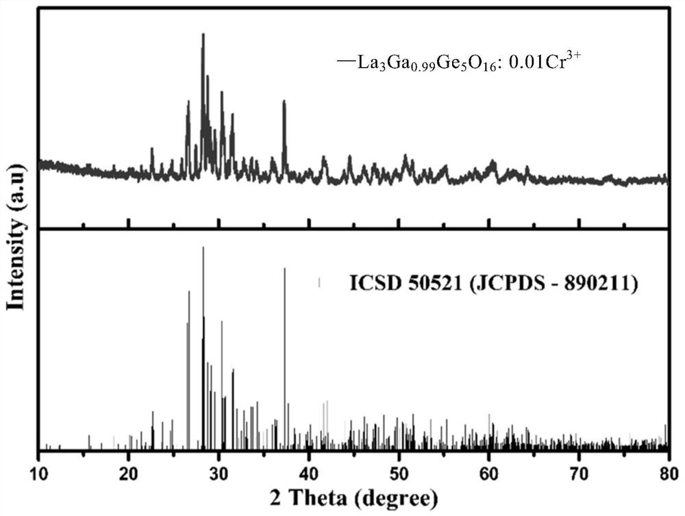
[0091] This embodiment provides a group of fluorescent materials whose general formula is La 3 Ga 1-y Ge 5 o 16 :yCr 3+ , where 0

[0092] La 3 Ga 0.995 Ge 5 o 16 :0.005Cr 3+

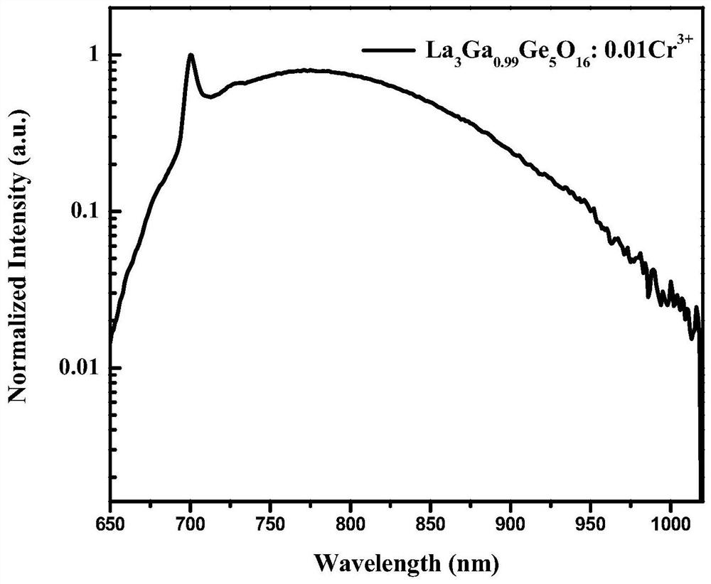
[0093] La 3 Ga 0.99 Ge 5 o 16 :0.01Cr 3+

[0094] La 3 Ga 0.97 Ge 5 o 16 :0.03Cr 3+

[0095] La 3 Ga 0.95 Ge 5 o 16 :0.05Cr 3+

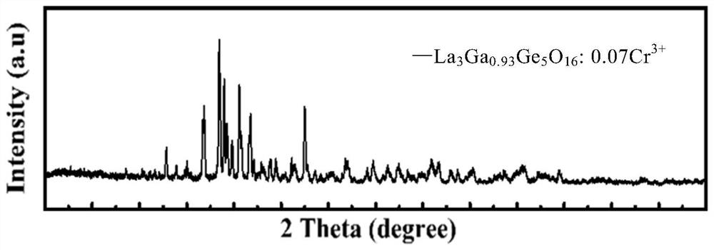
[0096] La 3 Ga 0.93 Ge 5 o 16 :0.07Cr 3+

[0097] La 3 Ga 0.91 Ge 5 o 16 :0.09Cr 3+

[0098] La 3 Ga 0.89 Ge 5 o 16 :0.11Cr 3+

[0099] La 3 Ga 0.87 Ge 5 o 16 :0.13Cr 3+

[0100] The preparation method of this group of fluorescent materials is: according to the stoichiometric ratio in the molecular formula of the fluorescent materials, accurately weigh the raw material La 2 o 3 , Ga 2 o 3 、GeO 2 and Cr 2 o 3 ;Put the weighed raw materials into an agate mortar and grind to mix evenly, then transfer the resulting mixture to an alumina crucibl...

Embodiment 2

[0105] This embodiment provides a fluorescent material with a molecular formula of La 2.97 Ga 0.99 Ge 5 o 16 :0.03Gd 3+ ,0.01Cr 3+ , the preparation method of the fluorescent material is as follows:

[0106] Accurately weigh the raw material La according to the stoichiometric ratio in the molecular formula of the fluorescent material 2 o 3 , Ga 2 o 3 、GeO 2 、Gd 2 o 3 and Cr 2 o 3 , put the weighed raw material into an agate mortar and grind it to mix evenly, then transfer the mixture to an alumina crucible, and place it in a tube furnace for sintering in an air atmosphere, controlling the sintering temperature to 1300°C The sintering time is about 6 hours, and after being cooled in the furnace, it is ground into powder to obtain fluorescent materials.

[0107] Such as Figure 5 As shown, the XRD diffraction pattern of the fluorescent material is compared with the standard X-ray diffraction pattern, and all the diffraction peaks of the fluorescent material are co...

Embodiment 3

[0111] This embodiment provides a fluorescent material whose molecular formula is La 2.97 Ga 0.99 Ge 5 o 16 :0.03Yb 3+ ,0.01Cr 3+ , the preparation method of the fluorescent material is as follows:

[0112] Accurately weigh the raw material La according to the stoichiometric ratio in the molecular formula of the fluorescent material 2 o 3 , Ga 2 o 3 、GeO 2 , Yb 2 o 3 and Cr 2 o 3 , put the weighed raw material into an agate mortar and grind it to mix evenly, then transfer the mixture to an alumina crucible, and place it in a tube furnace for sintering in an air atmosphere, controlling the sintering temperature to 1300°C The sintering time is about 6 hours, and after being cooled in the furnace, it is ground into powder to obtain fluorescent materials.

[0113] Such as Figure 7 As shown, the XRD diffraction pattern of the fluorescent material is compared with the standard X-ray diffraction pattern, and all the diffraction peaks of the fluorescent material are co...


PUM

PropertyMeasurementUnit
radiant fluxaaaaaaaaaa
wavelengthaaaaaaaaaa

Abstract

The invention provides a fluorescent material and a preparation method thereof, an optoelectronic device and a method for manufacturing the optoelectronic device. The fluorescent material has the following general formula: La 3(1‑x) Ga 1‑y Ge 5(1‑z) o 16 :3xA 3+ ,yCr 3+ ,5zB 4+ , wherein: x, y and z are not 0 at the same time; A represents at least one of Gd and Yb; B represents at least one of Sn, Nb and Ta. Under the excitation of blue visible light, purple visible light or ultraviolet light, the fluorescent material has an emission spectrum in the red visible light and near-infrared region, and has a wide reflection spectrum and high radiation flux, so it can be applied to optoelectronic devices such as LEDs. To meet the current application requirements of medical testing, food composition analysis, security cameras, iris / facial recognition, virtual reality, gaming notebooks, and laser detection and measurement.

Description

technical field [0001] The present invention relates to a fluorescent material and its preparation method, an optoelectronic device and a method for manufacturing the optoelectronic device, in particular to a fluorescent material with high radiation flux and wide emission wavelength in the red visible light-near infrared region and its preparation process, An optoelectronic device provided with the fluorescent material and a manufacturing process of the optoelectronic device. Background technique [0002] Visible light is the part of the electromagnetic spectrum that the human eye can perceive, and infrared light is electromagnetic waves (light) with longer wavelengths than visible light. Studies have shown that infrared light is able to "penetrate" into human skin, being absorbed by the epidermis, dermis and subcutaneous tissue. At the same time, the spectrum that some human organs can absorb is in the visible light range of the electromagnetic spectrum, while the reflecte...

Claims


Application Information

Patent Timeline
Patent Type & Authority Patents(China)
IPC IPC(8): C09K11/80H01L33/50
CPCC09K11/7707C09K11/7708C09K11/7775C09K11/7776H01L33/486H01L33/501H01L33/502C09K11/62C09K11/66C09K11/77C09K11/7766H01L33/005H01L2933/0041
Inventor 韦拉马尼·拉金德伦方牧怀刘如熹张合吕侊懋林晏申康桀侑盖伯瑞尔尼科洛·德·古斯曼胡淑芬
Owner EVERLIGHT ELECTRONICS
Why Eureka
Try Eureka