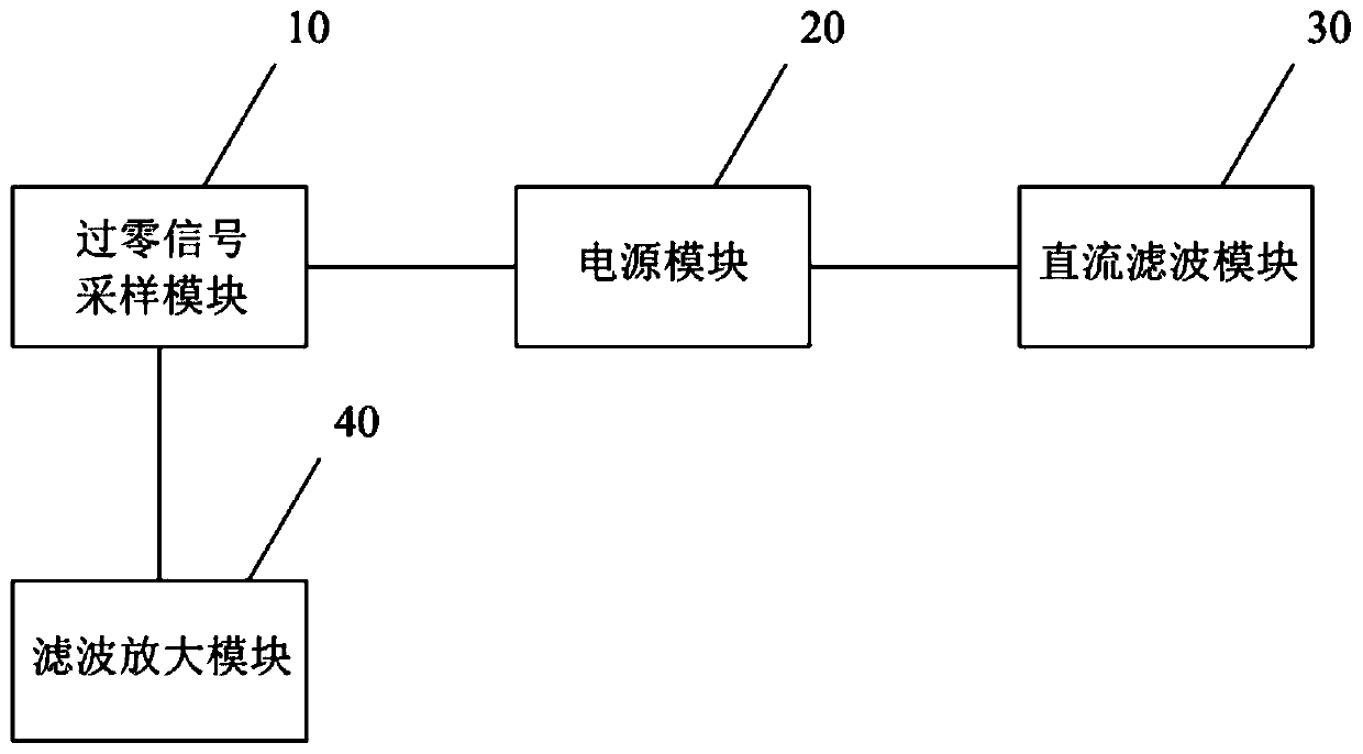
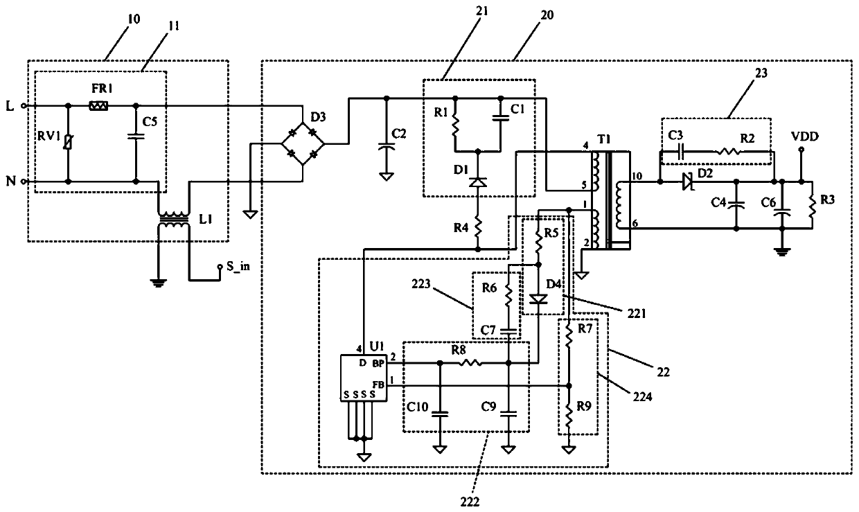
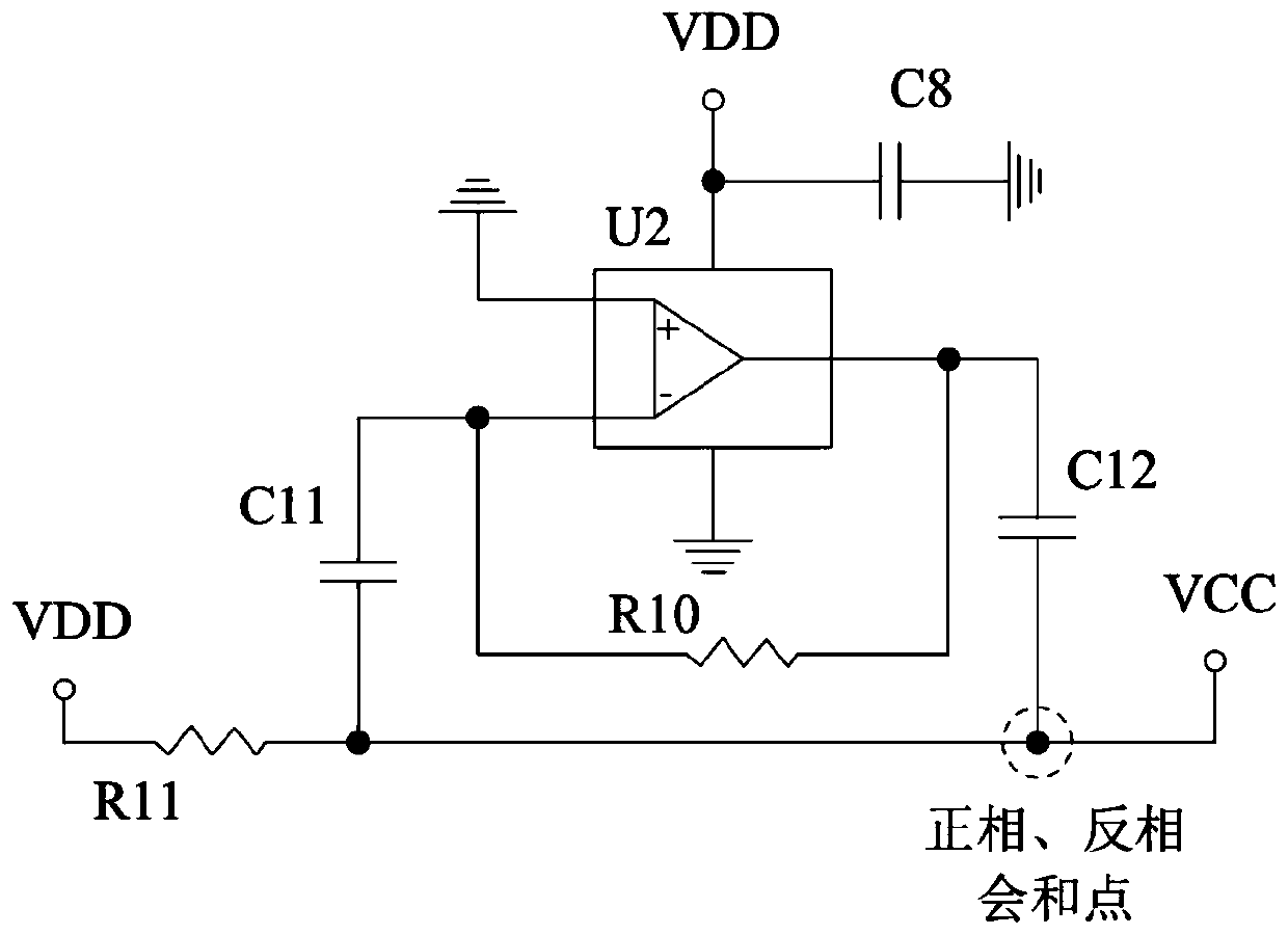
Zero-cross detection system
A zero-crossing detection and zero-crossing signal technology, applied in the direction of measuring electricity, measuring devices, measuring electrical variables, etc., can solve the problems of large loss, poor sampling consistency, sampling circuit delay, etc., to reduce ripple and avoid harmonics Interference, avoid delay effect
Pending Publication Date: 2019-06-28
深圳市闿思科技有限公司
0 Cites 2 Cited by
AI-Extracted Technical Summary
Problems solved by technology
[0004] For this reason, the purpose of the present invention is to propose a zero-crossing detectio...
Method used
By the establishment and verification of Pspice model, by simulation model, the reliability of verification circuit, the result shows, input the waveform of 1V, output only has the waveform of 140mV, and ripple and noise have only 2.9mV. In the actual verification board, the ripple noise of VCC is lower than 50mV (output 5V/1A), after filtering by the DC filter module 30, the ripple noise is reduced to below 5mV. In the application of this embodiment, set R10=R11, which is smaller than 100 ohms, and C11=C12, which is larger than 10uF. Therefore, the above-mentioned DC filtering module 30 has a very obvious effect in reducing ripple and noise.
Described anti-clutter interference circuit 42 comprises the second triode Q2, the 3rd triode Q3, the 21st resistance R21, the 22nd resistance R22, the 19th electric capacity C19, the twentieth electric capacity C20, the signal output by the fourth operational amplifier U4 is isolated and sampled by the second triode Q2, the twenty-first resistor R21, the twenty-second resistor R22, and the nineteenth capacitor C19 and the twentieth capacitor C20 form a two-stage π-type filter, which is used to control the conduction of the third triode Q3, so that the noise at the input end is filtered out. Since the noise is filtered out, the accuracy of the operational amplifier is affected. Requirements, you can choose an operational amplifier with lower precision to achieve signal amplification, thereby reducing the cost.
Described zero-crossing signal sampling module 10 comprises anti-lightning strike surge interference circuit 11 and mutual inductor L1, described anti-lightning strike surge interference circuit 11 is respectively connected with AC fire wire input terminal (L), AC neutral line input terminal (N ) and the primary winding of the transformer L1, the anti-lightning surge interference circuit 11 at least includes a safety capacitor C5, the primary winding of the transformer L1 and the safety capacitor C5 form a first filter circuit, so The primary winding of the transformer L1 is connected in series to the AC power grid. The prim...
Abstract
The invention discloses a zero-cross detection system. The system comprises a zero-cross signal sampling module, a power module and a direct current filtration module, wherein the zero-cross signal sampling module comprises a thunder-proof surge interference circuit and an inductor, the thunder-proof surge interference circuit is connected with an alternating current fire line input end, an alternating current zero line input end and a primary winding of the inductor and at least comprises a safety capacitor, the primary winding of the inductor and the safety capacitor constitute a first filtration circuit, and the primary winding of the inductor is connected to an alternating current grid in series; the power module comprises a bridge rectifier, a clamping circuit, a booster transformer and a primary side feedback system, the clamping circuit is connected with a second auxiliary winding of the booster transformer, a first auxiliary winding of the booster transformer is connected withthe primary side feedback system, and a buffer circuit is arranged on a secondary side winding of the booster transformer and a direct current voltage output end. The problems of delay of the samplingcircuit, poor sampling consistency and high loss can be solved.
Application Domain
Current/voltage measurementElectrical measurement instrument details +1
Technology Topic
CapacitancePower grid +12
Image
Examples
- Experimental program(1)
Example Embodiment
[0025] In order to make the above-mentioned objects, features and advantages of the present invention more obvious and understandable, the specific embodiments of the present invention will be described in detail below with reference to the accompanying drawings. Several embodiments of the invention are shown in the drawings. However, the present invention can be implemented in many different forms and is not limited to the embodiments described herein. On the contrary, the purpose of providing these embodiments is to make the disclosure of the present invention more thorough and comprehensive.
[0026] It should be noted that when an element is referred to as being "fixed to" another element, it can be directly on the other element or a central element may also exist. When an element is considered to be "connected" to another element, it can be directly connected to the other element or an intermediate element may be present at the same time. The terms "vertical", "horizontal", "left", "right", "upper", "lower" and similar expressions used herein are only for illustrative purposes, and do not indicate or imply the device or The element must have a specific orientation, be constructed and operated in a specific orientation, and therefore cannot be understood as a limitation of the present invention.
[0027] In the present invention, unless otherwise clearly specified and limited, the terms "installed", "connected", "connected", "fixed" and other terms should be understood in a broad sense, for example, it may be a fixed connection or a detachable connection , Or integrally connected; it can be a mechanical connection or an electrical connection; it can be directly connected or indirectly connected through an intermediate medium, and it can be the internal communication between two components. For those of ordinary skill in the art, the specific meanings of the above terms in the present invention can be understood according to specific circumstances. The term "and/or" as used herein includes any and all combinations of one or more related listed items.
[0028] See Figure 1 to Figure 4 , The zero-crossing detection system provided by an embodiment of the present invention includes a zero-crossing signal sampling module 10, a power supply module 20, and a DC filter module 30.
[0029] The zero-crossing signal sampling module 10 includes an anti-lightning surge interference circuit 11 and a transformer L1. The anti-lightning surge interference circuit 11 is respectively connected to the AC live wire input terminal (L), the AC neutral wire input terminal (N) and the The primary winding of the transformer L1 is connected, the anti-lightning surge interference circuit 11 includes at least a safety capacitor C5, the primary winding of the transformer L1 and the safety capacitor C5 form a first filter circuit, and the transformer The primary winding of L1 is connected to the AC grid in series. The primary winding of the transformer L1 and the safety capacitor group C5 form the first filter circuit, which can avoid the interference of harmonics. Since the primary winding of the transformer L1 is connected to the AC grid in series, there is almost no loss. When an AC signal passes through the winding, the current changes and it will be induced in the secondary winding. The signal induced by the secondary is S_in to avoid delay in the sampling circuit, regardless of whether the voltage AC at the AC live wire input terminal or the AC neutral wire input terminal is 85V or 265V, Or other values, as long as there is a very small current flowing through the transformer, a signal greater than uV level will be obtained in the secondary winding of the transformer, and the sampling consistency is good.
[0030] It should be pointed out that during the specific implementation, the AC live wire input terminal (L) and the AC neutral wire input terminal (N) can be interchanged without affecting the work flow.
[0031] Specifically, in this embodiment, the anti-lightning surge interference circuit 11 further includes a varistor RV1 and a fuse resistor FR1, and the varistor RV1 is connected to the AC live wire input (L) and the AC zero Between the line input terminals (N), the fuse resistor FR1 is connected between the AC live line input terminal (L) and the safety capacitor C5.
[0032] In addition, this embodiment also improves the transformer L1. Specifically, the magnetic core of the transformer L1 adopts an amorphous nano-magnetic ring with a diameter of 5.5mm and an inductance of 350uH. The winding adopts a composite material of 0.25mm. The composite material wire includes 95.5% Sn, 3% Ag, 1.5% Cu, the primary winding and the secondary winding of the transformer L1 are wound in the same phase for 50 times, and the inductance of the coil is 5uH. The transformer designed in this way has small size, high magnetic permeability, high squareness ratio and ideal high temperature stability.
[0033] The power supply module 20 includes a bridge stack D3, a clamping circuit 21, an adjusting transformer T1, and a primary feedback system 22. The bridge stack D3 is connected to the zero-crossing signal sampling module 10 and the clamping circuit 21, respectively. The clamping circuit 21 is connected to the second auxiliary winding (namely 4-5 ends) of the adjusting transformer T1, and the first auxiliary winding (namely 1-2 ends) of the adjusting transformer T1 is connected to the primary feedback system 22 Connected, the secondary winding (ie, terminals 6-10) of the adjusting transformer T1 outputs a DC voltage, and the secondary winding of the adjusting transformer T1 and the DC voltage output terminal VDD are provided with a buffer circuit 23 for reducing ripple and noise.
[0034] In the power module 20, the primary-side feedback system 22 can supplement the low power consumption effect during standby, and the buffer circuit 23 can reduce ripple and noise, thereby providing a reliable DC voltage with low ripple and low noise for the back end.
[0035] Specifically, the buffer circuit 23 includes a third capacitor C3 and a second resistor R2. The third capacitor C3 and the second resistor R2 are connected in series with the secondary winding of the adjusting transformer T1 and the DC voltage output terminal. Between VDD.
[0036] In this embodiment, the power module 20 further includes a second filter circuit, the second filter circuit specifically uses a second capacitor C2, the second filter circuit is connected to the bridge stack D3, and the clamping circuit 21 specifically includes A first resistor R1, a first capacitor C1, and a first diode D1, the first resistor R1 and the first capacitor C1 are connected in parallel between the bridge stack D3 and the cathode of the first diode D1 Meanwhile, the anode of the first diode D1 is connected to the second auxiliary winding of the adjusting transformer T1.
[0037] The primary feedback system 22 includes a rectifier circuit 221, a π-type filter circuit 222, a phase compensation circuit 223, a feedback circuit 224, and a control chip U1. The rectifier circuit 221 is connected to the first auxiliary winding of the adjustment transformer T1. The π-type filter circuit 222 is connected to the rectifier circuit 221 and the control chip U1, the phase compensation circuit 223 is connected between the π-type filter circuit 222 and the rectifier circuit 221, and the feedback circuit 224 is connected to The first auxiliary winding of the adjusting transformer T1 is connected to the control chip U1.
[0038] Specifically, the rectifier circuit 221 is composed of a fourth diode D4 and a fifth resistor R5, and the π-type filter circuit 222 is composed of an eighth resistor R8, a ninth capacitor C9, and a tenth capacitor C10, which are used for controlling The chip U1 provides a DC voltage to supplement the low power consumption effect during standby. The phase compensation circuit 223 is composed of a sixth resistor R6 and a seventh capacitor C7, and the feedback circuit 224 is composed of a seventh resistor R7 and a ninth resistor R9. .
[0039] The above-mentioned power module 20 has the advantages of low cost, high school rate, and low standby power consumption, and can provide a downstream MCU, OP, and other control units and radio frequency units with a reliable DC voltage with low ripple and low noise.
[0040] The DC filter module 30 is connected to the DC voltage output terminal VDD. When the output DC voltage is 5V and the current is 1A, the ripple and noise are less than 50mV, which is excellent in many applications. However, in the power supply of the RF unit and the analog front end, consider the receiving sensitivity of the RF signal and analog In signal amplification, a lower-noise power supply system is required, and a better active filter design is required. Therefore, the DC filter module 30 is also improved in this embodiment.
[0041] Specifically, the DC filter module 30 includes an active filter circuit composed of a tenth resistor R10, an eleventh resistor R11, an eleventh capacitor C11, a twelfth capacitor C12, and a second operational amplifier U2. Composition, the first end of the eleventh resistor R11 is connected to the DC voltage output terminal VDD, the second end of the eleventh resistor R11 is connected to the first end of the eleventh capacitor C11, the tenth The second terminal of a capacitor C11 is connected to the inverting input terminal of the second operational amplifier U2, the non-inverting input terminal of the second operational amplifier U2 is grounded, and the tenth resistor R10 is connected to the second operational amplifier U2. Between the inverting input terminal and the output terminal of the second operational amplifier U2, the first terminal of the twelfth capacitor C12 is connected to the output terminal of the second operational amplifier U2, and the first terminal of the twelfth capacitor C12 is The two ends are respectively connected to the second end of the eleventh resistor R11 and the first end of the eleventh capacitor C11.
[0042] Ripple and noise enter the inverting input port of the second operational amplifier U2 through the eleventh resistor R11 and the eleventh capacitor C11. The amplified output ripple and noise are in the opposite phase and pass through the twelfth capacitor C12. The dashed dots converge, and the AC signals that do not enter the positive phase of the eleventh capacitor C11 cancel each other out, and a VCC with smaller ripple and noise can be obtained. The calculation model is: V O =V i /[R10·R11·C11·C12·S 2 +R11·(C11+C12)·S+1], where V O Output ripple, noise, V i Is the input ripple and noise, and S is the calculated variable factor, which is determined according to the characteristics of different operational amplifiers. In this embodiment, the ripple and noise of the output DC VCC are less than 5mV, the output voltage is DC 5V, and the current is 1A.
[0043] Through the establishment and verification of the Pspice model and the simulation model to verify the reliability of the circuit, the results show that the input 1V waveform, the output is only 140mV, and the ripple and noise are only 2.9mV. In the actual verification board, the ripple noise of the VCC is lower than 50mV (output 5V/1A). After filtering by the DC filter module 30, the ripple noise is reduced to less than 5mV. In the application of this embodiment, set R10=R11, which is less than 100 ohms, and C11=C12, which is greater than 10uF. Therefore, the aforementioned DC filter module 30 has a very obvious effect in reducing ripple and noise.
[0044] Optionally, as a further optimization, the zero-crossing detection system of this embodiment further includes a filtering and amplifying module 40, the secondary winding of the transformer T1 is connected to the secondary inductive signal terminal S_in, and the filtering and amplifying module 40 and the The secondary sensing signal terminal S_in is connected.
[0045] Specifically, the filtering and amplifying module 40 includes a low-pass filter 41, a third operational amplifier U3, a fourth operational amplifier U4, and an anti-clutter interference circuit 42. The low-pass filter 41 and the third operational amplifier U3 The non-inverting input terminal of the third operational amplifier U3 is connected to the non-inverting input terminal of the fourth operational amplifier U4, and the input terminal of the fourth operational amplifier U4 is connected to the anti-clutter interference circuit 42.
[0046] Among them, the low-pass filter 41 is composed of a fifteenth capacitor C15, a twelfth resistor R12, and a fourteenth resistor R14.
[0047] The filtering and amplifying module 40 further includes a thirteenth capacitor C13, a seventeenth resistor R17, an eighteenth resistor R18, a seventeenth capacitor C17, a fourteenth capacitor C14, and a nineteenth resistor R19. The capacitor C13 serves as the decoupling capacitor of the third operational amplifier U3, the seventeenth resistor R17 serves as the negative feedback resistor of the third operational amplifier U3, the eighteenth resistor R18 and the seventeenth capacitor C17 The zero point compensation circuit of the third operational amplifier U3 is formed, the fourteenth capacitor C14 is used as the decoupling capacitor of the fourth operational amplifier U4, and the nineteenth resistor R19 is used as the negative of the fourth operational amplifier U4. Feedback resistance.
[0048] The fifteenth resistor R15 is used as the output load of the transformer L1. The filtering and amplifying module 40 obtains the sampled signal S_in of the transformer after sampling, and enters the operational amplifier U3 through the low-pass filter 41. At the same time, the twelfth resistor R12 and the fourteenth Resistor R14 divides VCC to U3 bias current and voltage, F hpass =1/[2π·C15·(R12||R14)] (high-pass filter cut-off frequency). C13 is the decoupling capacitor of U3, R17 is the negative feedback resistance of U3, R18 and C17 form the zero compensation circuit of U3, and the zero frequency is F Z1 =1/(2π·C17·R18), here set the zero frequency of the U3 op amp to 30Hz. The signal amplified by U3 enters the non-inverting end of U4 for amplification. C14 is the decoupling capacitor of U4, R19 is the negative feedback resistance of U4, C16 and R19 constitute the pole frequency F of U4 P1 =1/(2π·C16·R19), here set the pole frequency of U4 to 70Hz. C18 and R20 form the zero frequency F of U4 Z2 =1/(2π·C18·R20). Set the zero frequency of U4 to 40Hz here.
[0049] The anti-clutter interference circuit 42 includes a second transistor Q2, a third transistor Q3, a twenty-first resistor R21, a twenty-second resistor R22, a nineteenth capacitor C19, and a twentieth capacitor C20. The signal output by the fourth operational amplifier U4 is isolated and sampled by the second transistor Q2, the twenty-first resistor R21, the twenty-second resistor R22, the nineteenth capacitor C19, and the The twentieth capacitor C20 forms a two-stage π-type filter, which is used to control the conduction of the third transistor Q3, so as to filter out the noise at the input end. Because the noise is filtered out, the accuracy requirements of the operational amplifier can be Signal amplification can be achieved by selecting a lower precision operational amplifier, thereby reducing costs.
[0050] In addition, the above zero-crossing detection circuit can be designed as a complete ground plane at the bottom of the PCB during specific implementation to ensure that stray interference is avoided in the signal amplification system, and at the same time, there is better EMC. Each electronic device can be placed in The top layer of the PCB facilitates decoupling and good ground plane matching signals.
[0051] In addition, based on the above circuit structure, according to the signal acquisition waveform and the interference of clutter, test data with an oscilloscope, and consider the interference problem, this embodiment also provides an anti-interference filtering method, including:
[0052] Start;
[0053] Delay 5ms;
[0054] Start interrupt trigger;
[0055] Turn on the counter;
[0056] Calculate the time interval between adjacent rising edges;
[0057] Determine whether the time interval between two rising edges is greater than 1.5ms;
[0058] If yes, the trigger data is valid, then delay 5ms, turn on the IO port of output control, and control the output command; return
[0059] If not, return to the step of starting interrupt triggering.
[0060] In summary, in the above zero-crossing detection system, a stable and reliable zero-crossing signal can be obtained, and the sampling circuit has no loss, which can save loss and cost for the market in this application field, environmental protection, and low carbon. In addition, the low-noise power supply design can provide a power supply system with minimal noise in the field of smart IOT to power the radio frequency unit of the device, which improves the radio frequency performance and makes the interconnection of all devices more reliable connection, ensuring the stability of data transmission and avoiding The interference of clutter improves the receiving sensitivity of the radio frequency unit. In the neighborhood of small signal amplification, ordinary operational amplifiers can be used to achieve the characteristics of strong anti-interference ability, low noise amplification, low cost, stable and reliable performance.
[0061] It should be pointed out that the zero-crossing detection system provided by the present invention can be applied to system application fields that require strong anti-interference ability and zero-loss zero-crossing detection, can be applied to systems that require low-noise, high-efficiency power supply design, and can be applied It is necessary to use ordinary operational amplifiers to achieve low-noise amplification applications. For example, the amplification area of micro-volt signals in instruments and meters.
[0062] In the description of this specification, descriptions with reference to the terms "one embodiment", "some embodiments", "examples", "specific examples", or "some examples" etc. mean specific features described in conjunction with the embodiment or example , Structure, materials or features are included in at least one embodiment or example of the present invention. In this specification, the schematic representations of the above terms do not necessarily refer to the same embodiment or example. Moreover, the described specific features, structures, materials or characteristics may be combined in any one or more embodiments or examples in a suitable manner.
[0063] The above-mentioned embodiments only express several implementation modes of the present invention, and their description is more specific and detailed, but they should not be interpreted as a limitation on the patent scope of the present invention. It should be pointed out that for those of ordinary skill in the art, without departing from the concept of the present invention, several modifications and improvements can be made, and these all fall within the protection scope of the present invention. Therefore, the protection scope of the patent of the present invention should be subject to the appended claims.
PUM


Description & Claims & Application Information
We can also present the details of the Description, Claims and Application information to help users get a comprehensive understanding of the technical details of the patent, such as background art, summary of invention, brief description of drawings, description of embodiments, and other original content. On the other hand, users can also determine the specific scope of protection of the technology through the list of claims; as well as understand the changes in the life cycle of the technology with the presentation of the patent timeline. Login to view more.
Similar technology patents
Array chip mass spectrometry analysis method of photoelectrochemical reaction intermediate
InactiveCN110988100Ain situ analysisavoid delay
Owner:FUDAN UNIV
Shower head with rotary water outlet surface cover
Owner:KAIPING HANSHUN SANITARY WARE IND
High-strength steel plate quenching machining device
ActiveCN112063810AImprove quenching work efficiencyavoid delay
Owner:广州旺鑫机电设备有限公司
Semiconductor device
ActiveUS9076503B2increased operation speedavoid delay
Owner:LONGITUDE LICENSING LTD
Device and method for AC/UPS mixed networking
Owner:CHINA MOBILE GROUP DESIGN INST
Data access method and device, electronic equipment and storage medium
Owner:MIDEA GRP (SHANGHAI) CO LTD +1
Classification and recommendation of technical efficacy words
- Avoid harmonic interference
- avoid delay
Device and method for AC/UPS mixed networking
Owner:CHINA MOBILE GROUP DESIGN INST
Multi-radar remote monitoring system and method based on WebSocket
Owner:BEIHANG UNIV +1
Road paver with layer thickness measuring device
ActiveUS20120321386A1avoid delayfaster measurement result
Owner:JOSEPH VOEGELE AG
Laser hybrid welding method and laser hybrid welding torch using a zinc and/or carbon and/or aluminum-containing rod
InactiveUS8471173B2avoid delayreduced period of time
Owner:FRONIUS INTERNATIONAL GMBH
Method for autonomous measurement of pose of tripod structure of solar panel on non-cooperative spacecraft
InactiveCN104154919Aavoid delayavoid system instability
Owner:BEIJING UNIV OF POSTS & TELECOMM