Image sensor and manufacturing method and control method thereof

An image sensor and manufacturing method technology, applied in radiation control devices, etc., can solve problems such as image distortion, achieve the effect of improving imaging quality and reducing blooming phenomenon

Inactive Publication Date: 2019-06-28
HUAIAN IMAGING DEVICE MFGR CORP
View PDF6 Cites 5 Cited by
  • Summary
  • Abstract
  • Description
  • Claims
  • Application Information

AI Technical Summary

Problems solved by technology

[0004] Since the image signal of the image sensor comes from the photogenerated electrons generated by the photodiode absorbing the incident light, when high-intensity light irradiates the image sensor, the photogenerated electrons will exceed the full well capacity of the pixel and overflow into the adjacent pixels, causing blooming (light Halo) phenomenon, resulting in image distortion

Method used


Image

  • Image sensor and manufacturing method and control method thereof
  • Image sensor and manufacturing method and control method thereof
  • Image sensor and manufacturing method and control method thereof

Examples


Embodiment Construction

[0038] Specific implementations of the image sensor provided by the present invention, its manufacturing method, and its control method will be described in detail below in conjunction with the accompanying drawings.

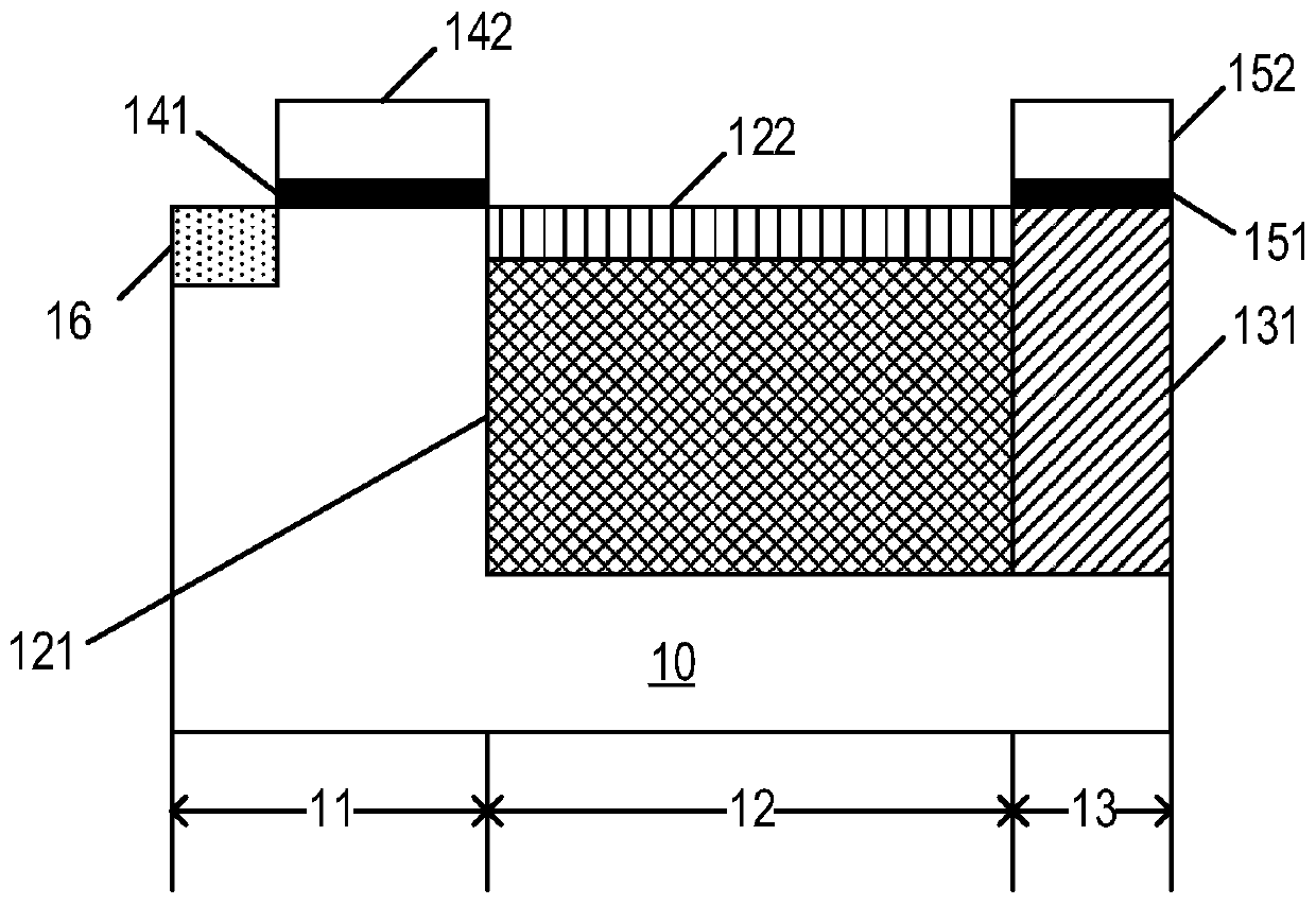
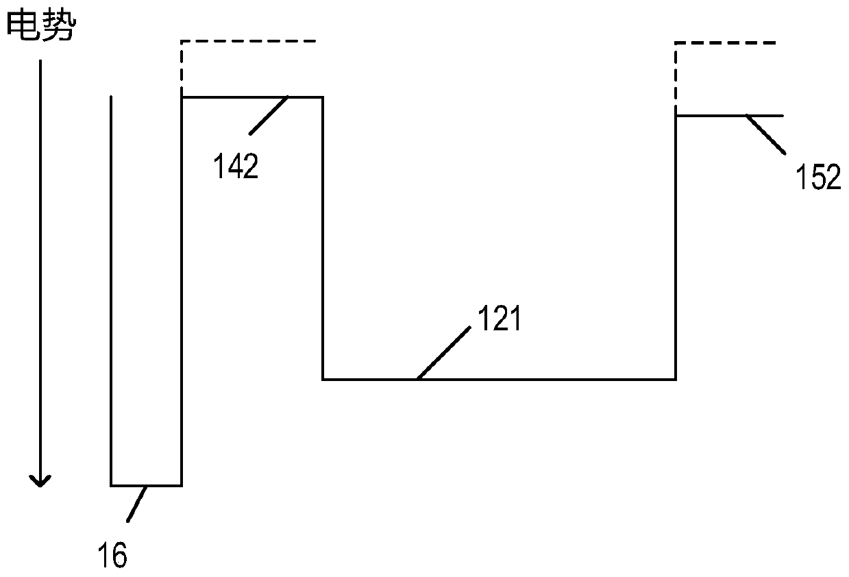
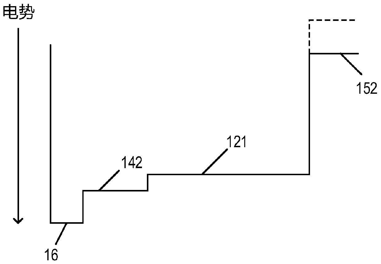
[0039] This specific embodiment provides an image sensor, with figure 1 It is a schematic structural diagram of a pixel unit in an image sensor in a specific embodiment of the present invention. Such as figure 1 As shown, the image sensor provided in this specific embodiment includes:

[0040] A substrate 10, the substrate 10 has a plurality of pixel units, the pixel unit includes a photoelectric doped region 12 and a transistor region 11 and an isolation region 13 located on opposite sides of the photoelectric doped region, the isolation region 13 is used to isolate the adjacent pixel units;

[0041] a transfer gate structure located on the surface of the substrate 10 and corresponding to the transistor region 11;

[0042] The bias electrode structure, loca...


PUM


Abstract

The invention relates to the technical field of semiconductor manufacturing, in particular to an image sensor and a manufacturing method and a control method thereof. The image sensor comprises a substrate which is provided with a plurality of pixel units, wherein each pixel unit comprises a photoelectric doping area, a transistor area and an isolation area which are located at the two opposite sides of the photoelectric doping area, and the isolation area is used for isolating the adjacent pixel units; a transmission grid structure which is located on the surface of the substrate and is corresponding to the transistor region; and a bias electrode structure which is located at the position, corresponding to the isolation region, of the surface of the substrate and used for increasing the potential barrier between the adjacent pixel units. The image sensor reduces the probability that photo-induced electrons in the photoelectric doped region overflow to the adjacent pixel units under strong light, and improves the imaging quality.

Description

technical field [0001] The invention relates to the technical field of semiconductor manufacturing, in particular to an image sensor, a manufacturing method and a control method thereof. Background technique [0002] The so-called image sensor refers to a device that converts optical signals into electrical signals. According to different principles, it can be divided into CCD (Charge Coupled Device, Charge Coupled Device) image sensor and CMOS (Complementary Metal-Oxide Semiconductor, metal oxide semiconductor element) image sensor. Since the CMOS image sensor is manufactured using a traditional CMOS circuit process, the image sensor and its required peripheral circuits can be integrated, so that the CMOS image sensor has a wider application prospect. [0003] According to different positions where light is received, CMOS image sensors can be classified into front-illuminated image sensors and back-side illuminated (Back Side Illumination, BSI) image sensors. Among them, ...

Claims


Application Information

Patent Timeline
Patent Type & Authority Applications(China)
IPC IPC(8): H01L27/146
Inventor 黄文军陈世杰黄晓橹
Owner HUAIAN IMAGING DEVICE MFGR CORP
Why Eureka
Try Eureka