A kind of black silicon material and preparation method thereof
A technology of black silicon and silicon substrate, which is applied in the field of black silicon materials and its preparation, can solve the problems of insufficient light trapping ability and affecting the light absorption rate of materials, and achieve uniformity and stability, uniform thickness distribution, and absorption rate-enhancing effect
- Summary
- Abstract
- Description
- Claims
- Application Information
AI Technical Summary
Benefits of technology
Problems solved by technology
Method used
Image

Examples
Embodiment 1
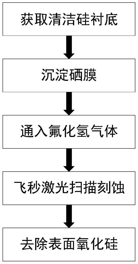
[0026] A method for preparing a black silicon material, the preparation path is as follows figure 1 shown, including the following steps:
[0027] Step 1: Obtain a Clean Silicon Substrate
[0028] Choose N-type high-resistance silicon as the substrate material, use the RCA standard cleaning method to clean the silicon substrate, then place the silicon substrate in 10% hydrofluoric acid solution for 10 seconds, and then ultrasonically rinse it with deionized water for 20 minutes , and blow-dried under a nitrogen atmosphere with a purity of 99.99%.
[0029] Step 2: Precipitating the Se film
[0030] Fix the clean silicon substrate obtained in step 1 on the walking unit of the vacuum chamber, take 0.2g of selenium powder with a purity of 99.99% as the evaporation source, evacuate the chamber to vacuum, adjust the workpiece speed to 15rad / min, and evaporate Current 70A, evaporation time 3min. After the precipitation is completed, the thickness of the selenium film deposited o...
Embodiment 2
[0038] A method for preparing a black silicon material, comprising the steps of:
[0039] Step 1: Obtain a Clean Silicon Substrate
[0040] Choose N-type high-resistance silicon as the substrate material, use the RCA standard cleaning method to clean the silicon substrate, then place the silicon substrate in 5% hydrofluoric acid solution for 20 seconds, and then ultrasonically rinse it with deionized water for 20 minutes , and blow-dried under a nitrogen atmosphere with a purity of 99.99%.
[0041] Step 2: Precipitating the Se film
[0042] Fix the clean silicon substrate obtained in step 1 on the walking unit of the vacuum chamber, take 0.2g of selenium powder with a purity of 99.99% as the evaporation source, evacuate the chamber to vacuum, adjust the workpiece speed to 15rad / min, and evaporate Current 50A, evaporation time 4min. After the precipitation is completed, the thickness of the selenium film deposited on the surface of the silicon substrate is 50nm.
[0043] St...
Embodiment 3
[0050] A method for preparing a black silicon material, comprising the steps of:
[0051] Step 1: Obtain a Clean Silicon Substrate
[0052] Choose N-type high-resistance silicon as the substrate material, use the RCA standard cleaning method to clean the silicon substrate, then place the silicon substrate in 8% hydrofluoric acid solution for 15 seconds, and then use deionized water to ultrasonically rinse it for 20 minutes , and blow-dried under a nitrogen atmosphere with a purity of 99.99%.
[0053] Step 2: Precipitating the Se film
[0054] Fix the clean silicon substrate obtained in step 1 on the walking unit of the vacuum chamber, take 0.2g of selenium powder with a purity of 99.99% as the evaporation source, evacuate the chamber to vacuum, adjust the workpiece speed to 15rad / min, and evaporate Current 80A, evaporation time 2min. After the precipitation is completed, the thickness of the selenium film deposited on the surface of the silicon substrate is 200nm.
[0055]...
PUM
| Property | Measurement | Unit |
|---|---|---|
| Thickness | aaaaa | aaaaa |
| Thickness | aaaaa | aaaaa |
| Thickness | aaaaa | aaaaa |
Abstract
Description
Claims
Application Information
 - R&D
- Intellectual Property
- Life Sciences
- Materials
- Tech Scout
- Unparalleled Data Quality
- Higher Quality Content
- 60% Fewer Hallucinations
Browse by: Latest US Patents, China's latest patents, Technical Efficacy Thesaurus, Application Domain, Technology Topic, Popular Technical Reports.
© 2025 PatSnap. All rights reserved.Legal|Privacy policy|Modern Slavery Act Transparency Statement|Sitemap|About US| Contact US: help@patsnap.com