Ultraviolet led epitaxial structure and its preparation method
An epitaxial structure, ultraviolet technology, applied in the direction of semiconductor devices, electrical components, circuits, etc., can solve problems such as degradation, low internal quantum efficiency, low light output power and efficiency, and achieve improved luminous efficiency, enhanced confinement, and enhanced radiation The effect of compounded chances
- Summary
- Abstract
- Description
- Claims
- Application Information
AI Technical Summary
Problems solved by technology
Method used
Image
Examples
Embodiment 1
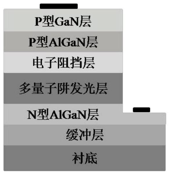
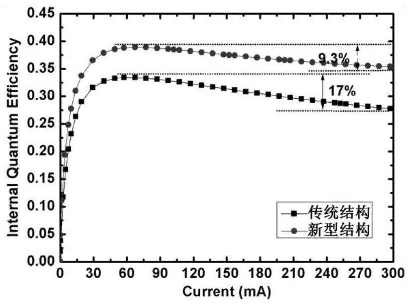
[0030] The first embodiment of the present invention provides an ultraviolet LED epitaxial structure, such as figure 1 As shown, it includes from bottom to top: substrate, buffer layer, N-type AlGaN layer, multi-quantum well light-emitting layer, electron blocking layer, P-type AlGaN layer and P-type GaN layer; figure 2 As shown, each quantum barrier layer in the multi-quantum well light-emitting layer includes a plurality of sublayers, preferably the number of sublayers is an odd number; the thickness of the sublayers and the content of aluminum molecules increase first according to the growth direction from bottom to top Post-decrement, increment and decrement boundary layers are located in the middle sublayers of each quantum barrier layer. The multi-quantum well light-emitting layer includes a plurality of quantum barrier layers, and the aluminum composition of the intermediate sublayers of the plurality of quantum barrier layers gradually increases from bottom to top acc...
Embodiment 2
[0034] The second embodiment of the present invention provides a method for preparing an ultraviolet LED epitaxial structure, including:
[0035] The sapphire substrate is placed in a metal organic compound chemical vapor deposition epitaxy reaction chamber, a hydrogen environment is set at a temperature of 1280°C, and the substrate is baked for 5 minutes;
[0036] A hydrogen environment is set at a temperature of 950-1200°C, and a buffer layer is grown on the substrate;
[0037] A hydrogen environment is set at a temperature of 1000°C-1200°C, and an N-type AlGaN layer is grown on the buffer layer;
[0038] A nitrogen environment is set at a temperature of 900-1000° C., and a multi-quantum well layer is grown on the N-type aluminum gallium nitride layer, and each quantum barrier layer in the multi-quantum well light-emitting layer includes a plurality of sublayers, and the sublayers are The thickness and the content of aluminum molecules increase first and then decrease accor...
PUM
| Property | Measurement | Unit |
|---|---|---|
| thickness | aaaaa | aaaaa |
| thickness | aaaaa | aaaaa |
| thickness | aaaaa | aaaaa |
Abstract
Description
Claims
Application Information


