
Waveguide feed substrate and preparation method thereof, antenna system and preparation method thereof

A waveguide feeding and antenna system technology, which is applied in the field of communication, can solve problems such as difficult integration, poor assembly accuracy, and loss, and achieve the effects of stable antenna system structure, reduced loss and error, and high process accuracy

Pending Publication Date: 2019-06-28
BEIJING BOE SENSOR TECH CO LTD +1
View PDF5 Cites 3 Cited by
  • Summary
  • Abstract
  • Description
  • Claims
  • Application Information

AI Technical Summary

Problems solved by technology

If the glass structure is integrated with the PCB structure, due to the material characteristics of the glass itself, it is not easy to integrate the PCB and other material substrates. It is necessary to add a fixed frame or other means to fix the two together, and the assembly accuracy is poor. High precision requirements are prone to large losses

Method used


Image

  • Waveguide feed substrate and preparation method thereof, antenna system and preparation method thereof
  • Waveguide feed substrate and preparation method thereof, antenna system and preparation method thereof
  • Waveguide feed substrate and preparation method thereof, antenna system and preparation method thereof

Examples


Embodiment 1

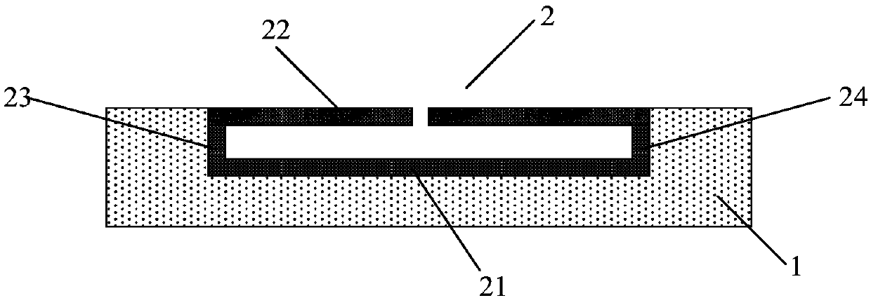
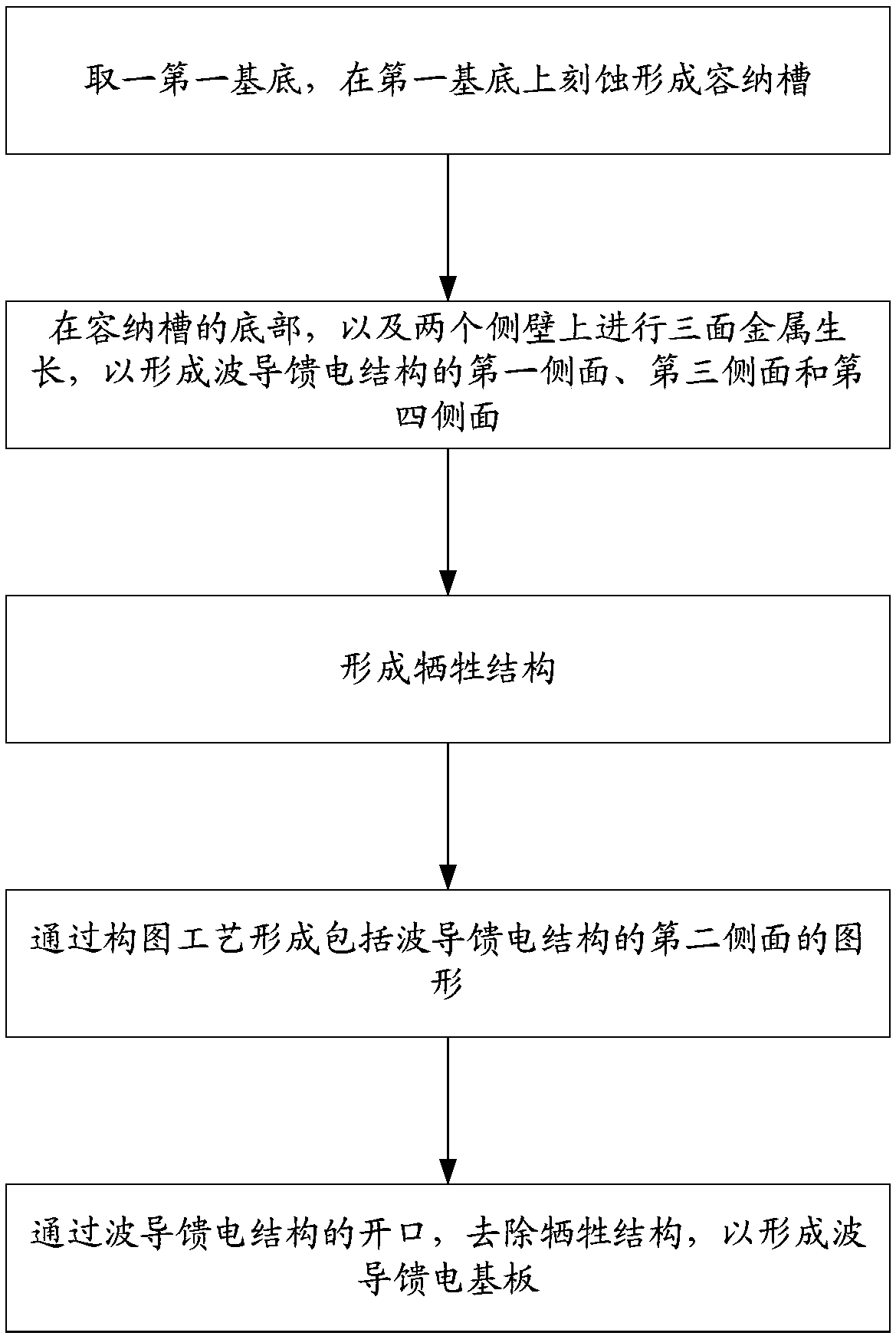
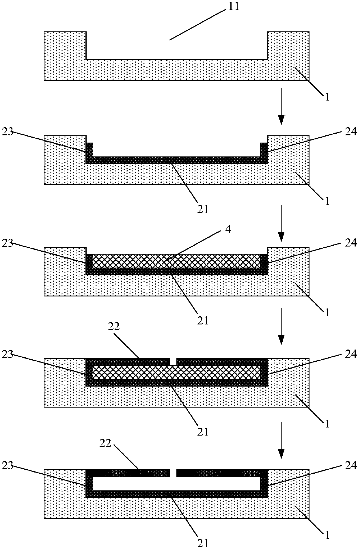
[0044] like figure 1 As shown, this embodiment provides a waveguide feeding substrate, including: a first substrate 1 and a waveguide feeding structure 2; wherein, there is a receiving groove 11 on the first substrate 1; the receiving groove 11 has a base, and is connected with the bottom The first side wall and the second side wall that are connected and oppositely arranged (that is, the receiving groove 11 is similar to a U-shaped groove); the waveguide feeding structure 2 is embedded in the receiving groove 11, and the waveguide feeding structure 2 is an internal hollow structure , which has a first surface 21 in contact with the bottom of the receiving tank, a second surface 22 opposite to the first surface 21, and a third surface 23 connected between the first surface 21 and the second surface 22 and oppositely disposed and the fourth surface 24; wherein, the third surface 23 is arranged on the first side wall of the receiving groove 11, the fourth surface 24 is arranged ...

Embodiment 2

[0069] like Image 6 As shown, this embodiment provides a waveguide feeding substrate, which is substantially the same as the waveguide feeding substrate in the embodiment, the difference is that a second surface 22 of the waveguide feeding structure 2 is provided with a second substrate.

[0070] When the waveguide feeding substrate and the antenna substrate in this embodiment are fixed together, the second substrate 3 of the waveguide feeding substrate and the substrate with the microstrip line in the antenna substrate can be fixed together through a bonding process. The precision is high, and the structure of the formed antenna system is stable, which can greatly reduce the loss and error caused by the mechanical assembly of the antenna system.

[0071] Wherein, the materials of the first substrate 1 and the waveguide feeding structure 2 in the waveguide feeding substrate of this embodiment can be the same materials as those in the first embodiment. The material of the se...


PUM


Abstract

The present invention provides a waveguide feed substrate and a preparation method thereof, an antenna system and a preparation method thereof, belonging to the technical field of communication. The waveguide feed substrate comprises a substrate having a holding groove comprising a bottom portion and a first side wall and a second side wall which are connected with the bottom portion and are oppositely arranged; a waveguide feed structure inlaid in the holding groove, being a hollow structure and having a first surface arranged at the bottom portion of the holding groove and a second surface relatively arranged with the first surface; and a third surface and a fourth surface which are connected between the first surface and the second surface and are oppositely arranged, wherein the thirdsurface is arranged on the first side wall, the second surface is arranged on the second side wall, and the second surface is provided with an opening. Therefore, the first substrate are fixed with the antenna substrate through a bonding process, the process is high in precision, the formed antenna system is stable in structure to greatly reduce the loss and errors of the antenna system caused bymechanical assembling.

Description

technical field [0001] The invention belongs to the technical field of communication, and in particular relates to a waveguide feeding substrate and a preparation method thereof, an antenna system and a preparation method thereof. Background technique [0002] At present, the feeding of liquid crystal antenna is mainly based on microstrip line feeding and substrate integrated waveguide (SIW) feeding. The microstrip line feed is characterized by greater isolation and higher integration, but the disadvantage is greater insertion loss. The substrate-integrated waveguide feeding feature is that it can replace the rectangular waveguide, and it is superior to the traditional rectangular metal waveguide in terms of cross-sectional size, loss characteristics, processing costs, and integration capabilities. , The upper and lower metal layers are plated, which is similar to the performance of metal waveguide, and the dielectric board is mostly PCB. If the glass structure is integrat...

Claims


Application Information

Patent Timeline
Patent Type & Authority Applications(China)
IPC IPC(8): H01Q1/50
CPCH01Q9/0457H01Q1/38H01P1/184H01P11/002H01Q1/50
Inventor 王瑛丁天伦武杰曹雪蔡佩芝车春城刘昊李亮贾皓程
Owner BEIJING BOE SENSOR TECH CO LTD
Features
  • Generate Ideas
  • Intellectual Property
  • Life Sciences
  • Materials
  • Tech Scout
  • Unparalleled Data Quality
  • Higher Quality Content
  • 60% Fewer Hallucinations
Learn More