
Display device

A technology for display devices and display areas, applied in nonlinear optics, instruments, optics, etc., can solve the problems of insufficient charging, high impedance, and the inability to realize narrow borders of the display panel 200', and achieve the effect of realizing ultra-narrow borders

Inactive Publication Date: 2019-07-05
TCL CHINA STAR OPTOELECTRONICS TECH CO LTD
View PDF5 Cites 14 Cited by
  • Summary
  • Abstract
  • Description
  • Claims
  • Application Information

AI Technical Summary

Problems solved by technology

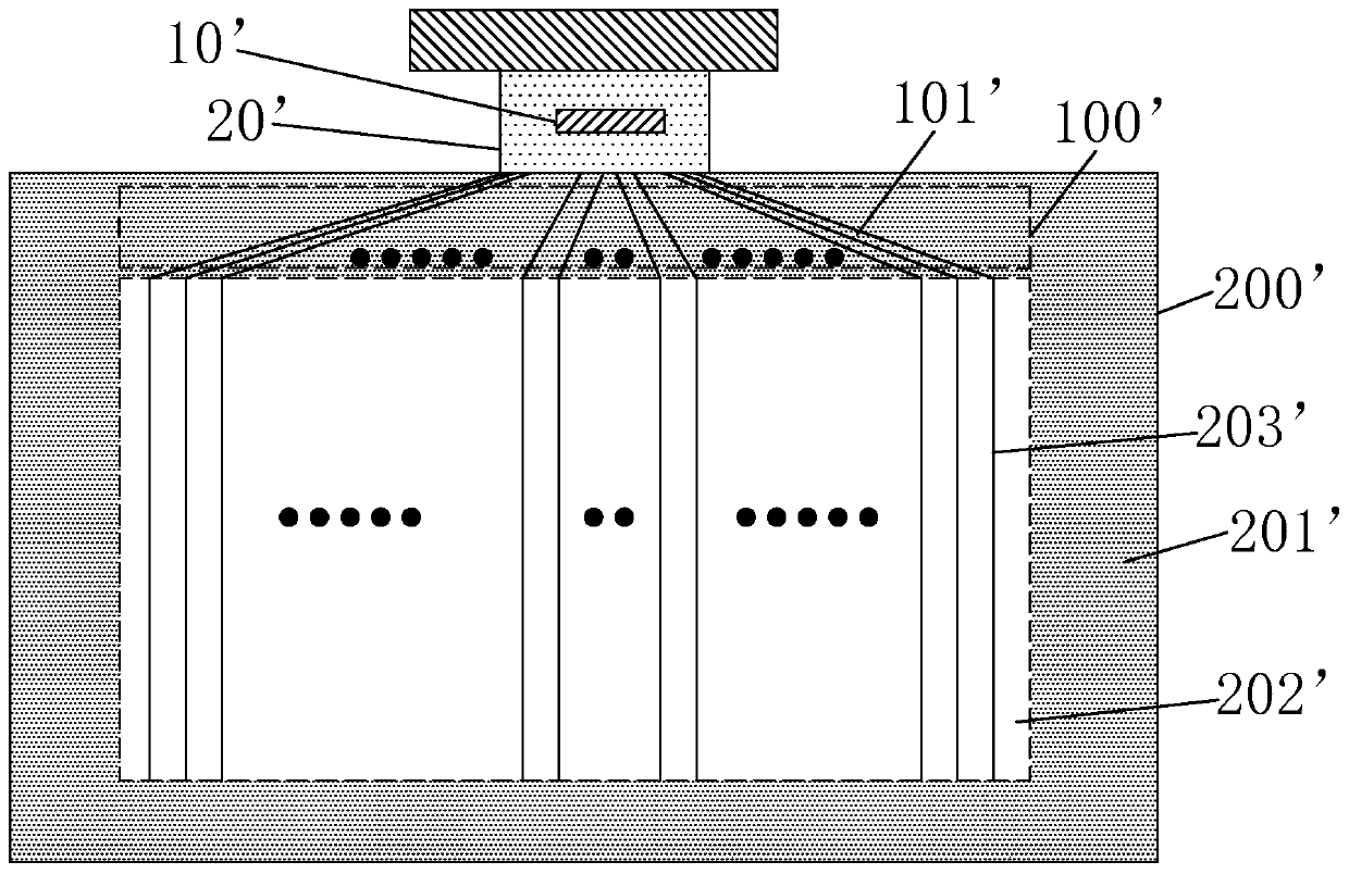
However, there are two problems in the existing fan-out area 100'. First, the fan-out area 100' is located in the non-display area 201' of the display panel 200'. Due to the existence of the fan-out area 100', the display panel 200' cannot achieve narrow border, secondly, in the fan-out area 100', the fan-out traces 101' located in the middle area of ​​the fan-out area 100' are relatively short, and the fan-out traces 101' located on both sides of the fan-out area 100' are relatively long, resulting in The impedance of the fan-out wiring 101' in the two sides of the out area 100' is higher than the impedance of the fan-out wiring 101' in the middle area, so that the data lines 203' transmitted to the areas on both sides of the display area 202' of the display panel 200' Compared with the signal attenuation of the data line 203' transmitted to the middle area of ​​the display area 202', the signal attenuation is serious, which eventually leads to a serious insufficient charging problem in the areas on both sides of the display area 202' compared with the middle area, which is visually manifested as color shift

Method used


Image

  • Display device
  • Display device
  • Display device

Examples


Embodiment Construction

[0025] In order to further illustrate the technical means adopted by the present invention and its effects, the following describes in detail in conjunction with preferred embodiments of the present invention and accompanying drawings.

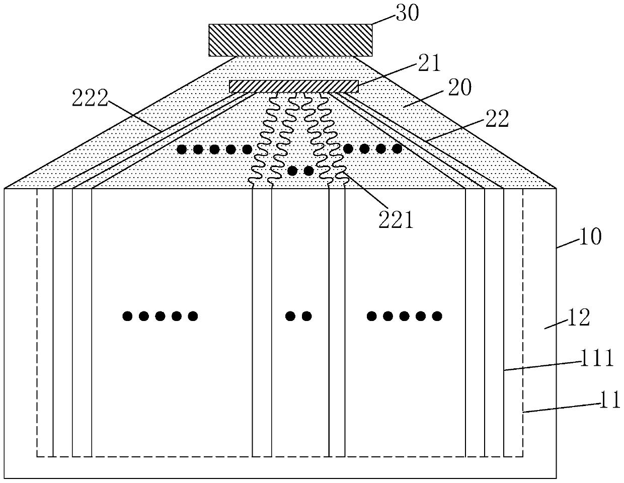
[0026] see figure 2 , the present invention provides a display device, comprising: a display panel 10 and a chip-on-chip film 20 connected to the display panel 10;

[0027] The display panel 10 includes a display area 11 and a non-display area 12 surrounding the display area 11; the display area 11 is provided with a plurality of data lines 111 distributed at intervals;

[0028] The COF 20 is provided with a source driver chip 21 and a plurality of fan-out wirings 22 connected to the source driver chip 21 at one end; the other ends of the plurality of fan-out wirings 22 are respectively connected to a plurality of data lines 11 one-to-one correspondence connection.

[0029] It should be noted that the fan-out wiring 22 connecting the source...


PUM


Abstract

The invention provides a display device comprising a display panel and a chip on film connected to the display panel, wherein the display panel comprises a display area and a non-display area surrounding the display area; the display area is provided with a plurality of spaced data lines; the chip on film is provided with a source driving chip and a plurality of fan-out wires connected to the source driving chip at one ends; the other ends of the plurality of fan-out wires are respectively connected to the plurality of data lines correspondingly, and the plurality of fan-out wires form a sector-shaped area. Equivalent to setting the fan-out area of the prior art on the chip on film, the portion near the chip on film of the non-display area of the display panel can be made narrower to achieve an ultra-narrow border of the display panel.

Description

technical field [0001] The present invention relates to the field of display technology, in particular to a display device. Background technique [0002] Thin Film Transistor (TFT) is the main driving element in current Liquid Crystal Display (LCD) and Active Matrix Organic Light-Emitting Diode (AMOLED). It is related to the display performance of the flat panel display device. [0003] Most of the liquid crystal displays currently on the market are backlight liquid crystal displays, which include a liquid crystal display panel and a backlight module. The working principle of the liquid crystal display panel is to pour liquid crystal molecules between the thin film transistor array substrate (ThinFilm Transistor Array Substrate, TFT Array Substrate) and the color filter (ColorFilter, CF) substrate, and apply pixel voltage on the two substrates respectively. and the common voltage, through the electric field formed between the pixel voltage and the common voltage to control...

Claims


Application Information

Patent Timeline
Patent Type & Authority Applications(China)
IPC IPC(8): G02F1/1345
CPCG02F1/13452G02F1/13454G02F1/136286
Inventor 傅晓立
Owner TCL CHINA STAR OPTOELECTRONICS TECH CO LTD
Learn More