Array substrate, display panel and electronic device
A technology for array substrates and display panels, applied in nonlinear optics, instruments, optics, etc., can solve problems such as complex multi-domain pixels
- Summary
- Abstract
- Description
- Claims
- Application Information
AI Technical Summary
Problems solved by technology
Method used
Image


Examples
Embodiment 1
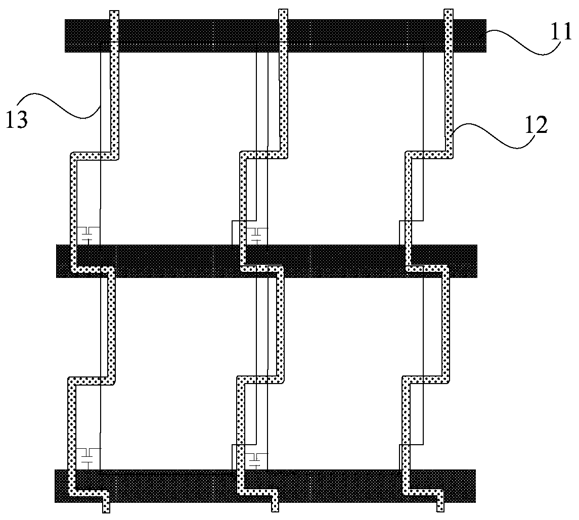
[0040] image 3 is a schematic structural diagram of an array substrate provided in Embodiment 1 of the present invention, Figure 4 is a schematic cross-sectional structure diagram of an array substrate provided in Embodiment 1 of the present invention, Figure 5 is a schematic cross-sectional structure diagram of a display panel formed by an array substrate provided in Embodiment 1 of the present invention, Figure 8 It is a pixel simulation diagram of an array substrate provided in Embodiment 1 of the present invention, Figure 9 It is a color shift degree map of pixels of an array substrate provided in Embodiment 1 of the present invention.
[0041] An embodiment of the present invention provides an array substrate 10 for forming a display panel with an opposite substrate 20, specifically, as Figure 3 to Figure 5 As shown, the array substrate 10 and the opposite substrate 20 are arranged in a box, and the array substrate 10, the opposite substrate 20 and the layer of l...
Embodiment 2
[0055] Figure 10 It is a schematic cross-sectional structure diagram of a display panel provided by Embodiment 2 of the present invention.
[0056] An embodiment of the present invention provides a display panel, including an array substrate 10, an opposite substrate 20, and a liquid crystal molecule layer located between the array substrate 10 and the opposite substrate 20, wherein the array substrate 10 and the opposite substrate 20 are arranged in a box, The substrate of the array substrate 10 is covered with a pixel electrode 13, and the base of the opposite substrate 20 is covered with a common electrode 21, and the pixel electrode 13 and the common electrode 21 are oppositely arranged, and the liquid crystal molecular layer is located between the pixel electrode 13 and the common electrode 21. , and the pixel area 14 is divided into a main pixel area 141 and a sub-pixel area 142 , the specific division method can refer to the first embodiment, which will not be repeated...
Embodiment 3
[0073] An embodiment of the present invention provides an electronic device, including any display panel in the above embodiments, the electronic device may be a liquid crystal display device, electronic paper, mobile phone, tablet computer, TV, notebook computer, digital photo frame, navigator, etc. Any product or part that has a display function.
[0074] An electronic device provided in this embodiment includes a display panel, the display panel includes an array substrate, an opposite substrate, and a liquid crystal molecular layer located between the array substrate and the opposite substrate, the array substrate is covered with pixel electrodes, and the opposite side The substrate is covered with a common electrode, and the display panel includes a first area corresponding to the main pixel area of the array substrate and a second area corresponding to the sub-pixel area of the array substrate, and one of the first area and the second area The distance between the pi...
PUM
 Abstract
Description
Claims
Application Information