Supercharge Your Innovation With Domain-Expert AI Agents!

Packaging process of LED display screen with double-layer glue-sealed laminated structure

A technology of LED display and packaging technology, which is applied in the field of display, can solve the problems of LED short circuit, module deformation, and uniform color of the whole screen, etc., and achieve the effects of thermal conductivity, moisture resistance, enhanced adhesion, and good thermal conductivity

Active Publication Date: 2019-07-16
深圳市宇帮电子有限公司
View PDF3 Cites 12 Cited by
  • Summary
  • Abstract
  • Description
  • Claims
  • Application Information

AI Technical Summary

Problems solved by technology

[0003] Among them, the LED display screen is composed of red, green and blue three-color LED light-emitting lamp beads spliced ​​to form a module panel, which is used to display various information such as text, images, videos, and videos. Various places, therefore, the LED display screen needs to have good heat dissipation effect, uniform flatness, consistent color of the whole screen, anti-collision, and moisture-proof and waterproof effect in the environment with high humidity. However, the LED display screen of the existing mounting process, Due to the ink color of the PCB, it is impossible to make the whole screen have the same color before it is lit. Some companies potted product modules are seriously deformed, and unpotted products are prone to moisture, resulting in LED short circuits. When the product is installed, the side of the module is easy to collide with the lamp bead

Method used


Image

  • Packaging process of LED display screen with double-layer glue-sealed laminated structure
  • Packaging process of LED display screen with double-layer glue-sealed laminated structure
  • Packaging process of LED display screen with double-layer glue-sealed laminated structure

Examples


Embodiment Construction

[0028] In order to express the present invention more clearly, the present invention will be further described below in conjunction with the accompanying drawings.

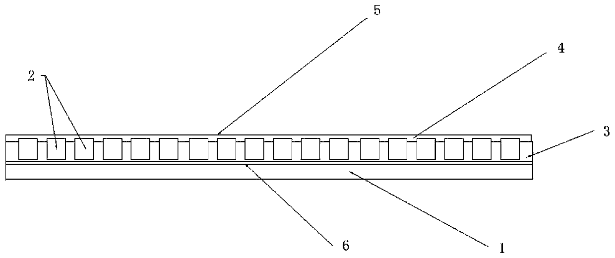
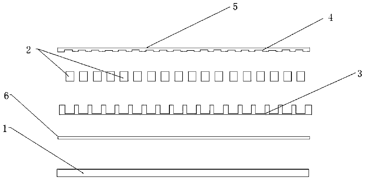
[0029] see Figure 1-Figure 3 , in order to achieve the above object, the present invention provides a LED display screen with a double-layer sealing structure, the LED display screen includes a circuit board 1 and LED light beads 2 mounted on the circuit board, and also includes The gap between the surface of 1 and the LED light bead 2 is filled with the first glue layer 3, and the upper surface of the LED light bead 2 is flush with the first glue layer 3 to form a flat surface; the upper surface of the first glue layer 3 is covered with the first glue layer Two adhesive layers 4 , and the hardness of the first adhesive layer 3 is less than that of the second adhesive layer 4 . And it is completed through the following packaging process:

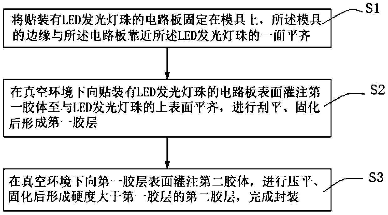
[0030] S1 Preparation before packaging: Fix the circuit board mounted wi...


PUM


Abstract

The invention discloses a packaging process of an LED display screen with a double-layer glue-sealed laminated structure. The packaging process comprises the following steps: a circuit board attachedwith an LED light-emitting lamp bead is fixed on a mold, and the edge of the mold is flush with one surface, close to the LED light-emitting lamp bead, of the circuit board; first glue is poured intothe surface of the circuit board attached with the LED light-emitting lamp bead in a vacuum environment until the surface of the circuit board is flush with the upper surface of the LED light-emittinglamp bead, and leveling and curing are carried out to form a first glue layer; and second glue is poured into the surface of the first glue layer in the vacuum environment, and flattening and curingare carried out to form a second glue layer harder than the first glue layer, thereby finishing the packaging. By carrying out two-time glue filling, the first glue layer and the second glue layer areformed, and the hardness of the first glue layer is smaller than the hardness of the second glue layer, so that the first glue layer of an LED display module after packaging is good in thermal conductivity, reduces the bottom ink color of the PCB and prevents damp and deformation, and the second glue layer plays a role in reinforcement and collision prevention.

Description

technical field [0001] The invention relates to the technical field of display screens, in particular to a packaging process for an LED display screen with a double-layer sealing glue structure. Background technique [0002] In recent years, LED (Light Emitting Diode, light-emitting diode) lamps have developed rapidly due to their advantages such as fast response, high brightness, long life, energy saving and environmental protection. [0003] Among them, the LED display screen is composed of red, green and blue three-color LED light-emitting lamp beads spliced ​​to form a module panel, which is used to display various information such as text, images, videos, and videos. Various places, therefore, the LED display screen needs to have good heat dissipation effect, uniform flatness, consistent color of the whole screen, anti-collision, and moisture-proof and waterproof effect in the environment with high humidity. However, the LED display screen of the existing mounting proce...

Claims


Application Information

Patent Timeline
IPC IPC(8): H01L33/54H01L33/56
CPCH01L33/54H01L33/56H01L2933/005
Inventor 吴宇嘉
Owner 深圳市宇帮电子有限公司
Features
  • R&D
  • Intellectual Property
  • Life Sciences
  • Materials
  • Tech Scout
  • Unparalleled Data Quality
  • Higher Quality Content
  • 60% Fewer Hallucinations
Learn More