Vapor phase decomposition device for semiconductor wafer pollutant measurement apparatus and door opening and closing device

a pollutant measurement and vapor phase decomposition technology, which is applied in the direction of measurement devices, instruments, specific gravity measurement, etc., can solve the problems of unnecessari influence of the conventional structure of the process chamber on the transfer unit, affecting the performance and yield of semiconductor devices, etc., and achieves the effect of keeping cleanness

Inactive Publication Date: 2009-10-08
KOREA TECH CO LTD
View PDF6 Cites 29 Cited by
  • Summary
  • Abstract
  • Description
  • Claims
  • Application Information

AI Technical Summary

Benefits of technology

[0014]To overcome inconveniences of the conventional art, it is an object of the present invention to provide an independent vapor phase decomposition (VPD) device, in which the VPD device is separated from the other devices in a semiconductor wafer pollutant measurement apparatus which is called an auto scanning system for measuring a pollution level of the wafer surface, to thus decompose the pollution level of the wafer surface using hydrofluoric acid (HF) and keep cleanness by N2 gas.

Problems solved by technology

As a result, various kinds of pollutants that are adsorbed on the surfaces of wafers affect performance and yield of semiconductor devices.
However, there is a problem that the conventional structure of the process chamber unnecessarily influences the transfer unit, the loader unit, the scanning unit, the dry unit, etc., in the process of decomposing the surface of the wafer gathered as a sample for measuring a pollution level of a wafer.

Method used


Image

  • Vapor phase decomposition device for semiconductor wafer pollutant measurement apparatus and door opening and closing device
  • Vapor phase decomposition device for semiconductor wafer pollutant measurement apparatus and door opening and closing device
  • Vapor phase decomposition device for semiconductor wafer pollutant measurement apparatus and door opening and closing device

Examples


Embodiment Construction

[0040]Hereinbelow, a vapor phase decomposition (VPD) device for a semiconductor wafer pollutant measurement apparatus which is called an auto scanning system, and a door opening and closing device thereof, according to the present invention will be described with reference to the accompanying drawings. Like reference numerals are assigned for like elements in the drawings.

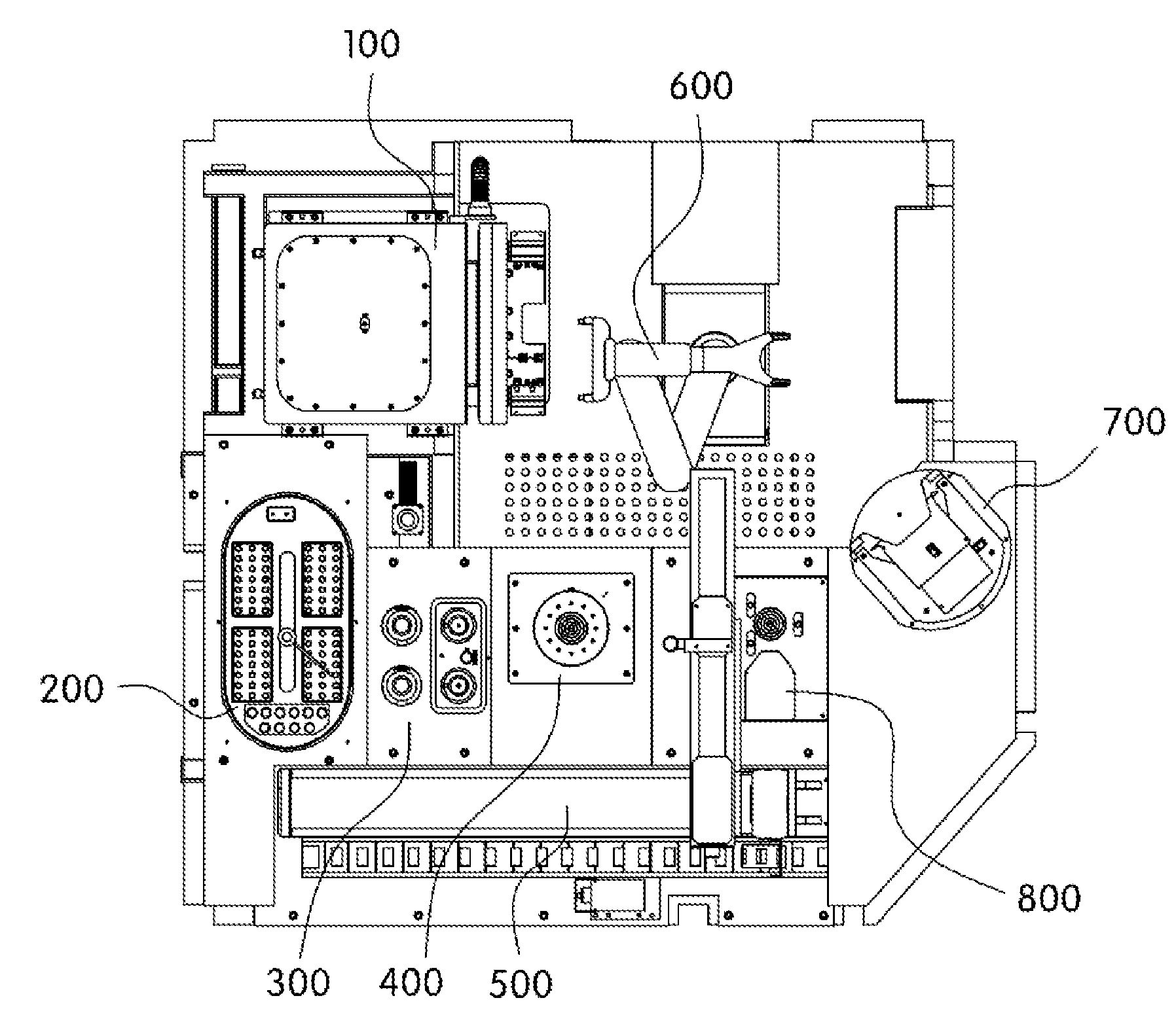
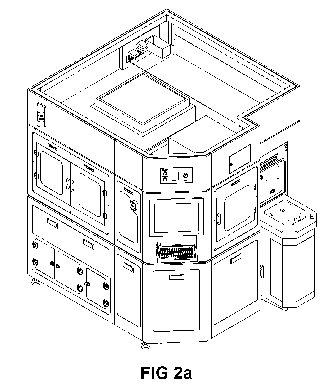
[0041]FIG. 2A is a perspective view showing the whole external appearance of a semiconductor wafer pollutant measurement apparatus to which a vapor phase decomposition (VPD) device is applied, and FIG. 2B is a schematic plan view showing the inside of the semiconductor wafer pollutant measurement apparatus of FIG. 2A.

[0042]As shown in FIGS. 2A and 2B, a vapor phase decomposition (VPD) device for a semiconductor wafer pollutant measurement apparatus according to the present invention, includes: an opener 700 which is located at an entrance portion in a space which is isolated from the outside portion, and opens a wa...


PUM

PropertyMeasurementUnit
sizeaaaaaaaaaa
sizeaaaaaaaaaa
sizeaaaaaaaaaa

Abstract

Provided is a vapor phase decomposition (VPD) device for a semiconductor wafer pollutant measurement apparatus and a door opening and closing device thereof. The VPD device includes: a rectangular vessel-shaped main body of the VPD device and a door which covers in a sealed form or opens the wafer inlet of the VPD device. Here, a predetermined space is formed in the inner portion of the rectangular vessel-shaped main body, support plates are formed on the bottom of the rectangular vessel-shaped main body and gas discharge and suction nozzles are located therein. In addition, a transparent see-through window is formed on the upper surface of the rectangular vessel-shaped main body, a detection electrode for controlling an inner atmosphere is formed at the center of the transparent see-through window, and one side surface of the rectangular vessel-shaped main body is opened to thus form a wafer inlet for introducing a wafer. The door opening and closing device includes: a forward and backward movement unit having cylinder loads, air cylinders, and plates, to make the door move forward and backward in order to open and close the wafer inlet of the main body of the VPD device; and an ascent and descent movement unit having a fixed plate, guide bars, a slide block, and a cylinder.

Description

CROSS-REFERENCE TO RELATED APPLICATION[0001]This application claims the benefit of Korean Patent Application No. 10-2008-0031128, filed on Apr. 3, 2008, in the Korean Intellectual Property Office, the disclosure of which is incorporated herein by reference.BACKGROUND OF THE INVENTION[0002]1. Field of the Invention[0003]The present invention relates to a vapor phase decomposition (VPD) device for a semiconductor wafer pollutant measurement apparatus which is called an auto scanning system, and a door opening and closing device thereof, in which the semiconductor wafer pollutant measurement device scans components having sticked on the surface of a silicon wafer with a liquid sample, and thus measures a pollution level using the liquid sample.[0004]2. Description of the Related Art[0005]In general, as a semiconductor device is high-integrated, various kinds of pollutants that are produced in semiconductor manufacturing lines and semiconductor manufacturing processes are adsorbed on th...

Claims


Application Information

Patent Timeline
Patent Type & Authority Applications(United States)
IPC IPC(8): G01N33/00
CPCH01L21/67126H01L21/67772H01L21/67748H01L21/6719H01L21/02
Inventor KIM, HO JINKIM, HYOUNG BAE
Owner KOREA TECH CO LTD
Why Eureka
Try Eureka