An electronic device and its antenna

An electronic device and antenna technology, applied in the field of wireless radio frequency, can solve the problems of high flatness and space requirements of antenna brackets, low space utilization rate of FPC antennas, and difficulty in using FPC antennas, so as to increase the overall structural strength and reliability, and save energy. Thickness direction space, the effect of saving thickness space

Active Publication Date: 2021-07-13
GEER TECH CO LTD
View PDF11 Cites 0 Cited by
  • Summary
  • Abstract
  • Description
  • Claims
  • Application Information

AI Technical Summary

Problems solved by technology

At present, the common antenna implementation method is FPC (Flexible Printed Circuit Board) antenna. The technical cost of FPC antenna is relatively low, and the process is relatively simple, but the flatness and space requirements of the antenna bracket are relatively high, and there are many ribs and area on the antenna bracket. FPC antennas cannot be used in small places
Therefore, the space utilization rate of the FPC antenna is low, which is not conducive to the use in the environment with complex antenna structure and small space
[0003] To sum up, how to effectively solve the problem that the FPC antenna is difficult to use in a small space environment is a problem that those skilled in the art need to solve

Method used


Image

  • An electronic device and its antenna
  • An electronic device and its antenna
  • An electronic device and its antenna

Examples


Embodiment Construction

[0025] The embodiment of the invention discloses an antenna of an electronic device, so as to meet the space limitation, structural strength and reliability requirements of the electronic product for the antenna.

[0026] The following will clearly and completely describe the technical solutions in the embodiments of the present invention with reference to the accompanying drawings in the embodiments of the present invention. Obviously, the described embodiments are only some, not all, embodiments of the present invention. Based on the embodiments of the present invention, all other embodiments obtained by persons of ordinary skill in the art without making creative efforts belong to the protection scope of the present invention.

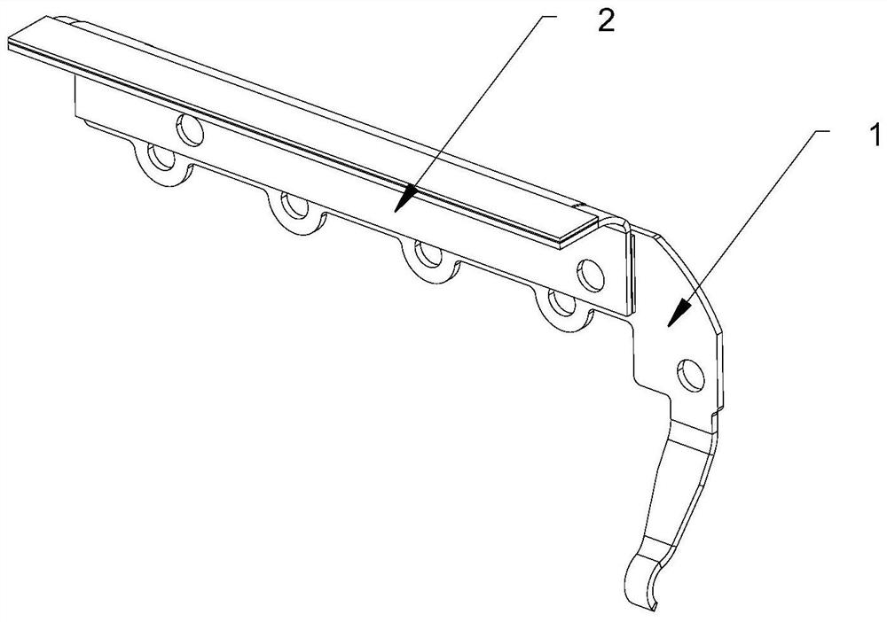
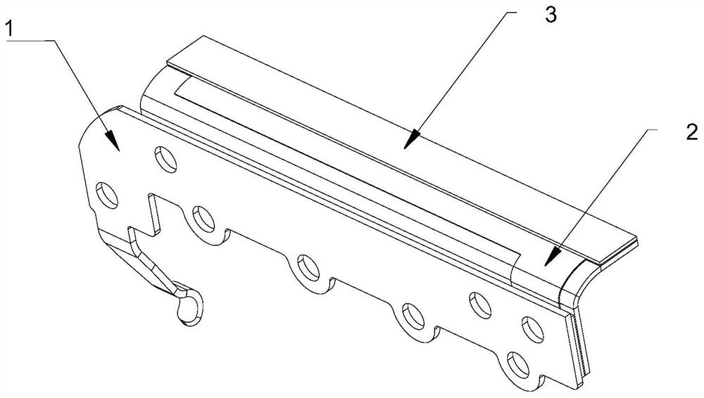
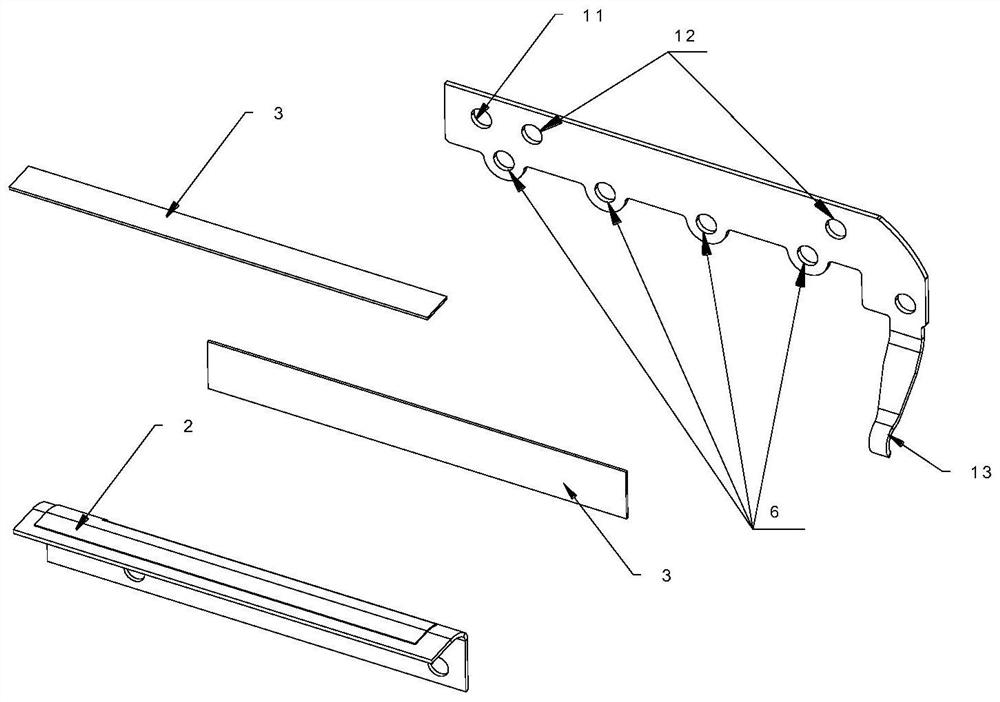
[0027] see Figure 1-Figure 3 , figure 1 It is a schematic diagram of the front structure of an antenna of an electronic device according to a specific embodiment of the present invention; figure 2 for figure 1 Schematic diagram of the back stru...


PUM


Abstract

The invention discloses an electronic device and its antenna, including a sheet metal stamping antenna and an FPC antenna. At least part of the FPC antenna is attached and fixedly connected to the sheet metal stamping antenna. The FPC antenna and the sheet metal stamping antenna are welded or surface assembled. conduction. Applying the electronic equipment and antenna provided by the present invention, a part of the antenna is made of FPC antenna, and the other part is made of sheet metal parts. Since the FPC antenna can be bent, the internal space of the electronic device can be fully utilized. The sheet metal stamping antenna has high strength, thickness The advantage of thinness can save thickness space, and the mixed process antenna provided by the present invention combines the advantages of both. It can not only improve the performance of the antenna through the FPC antenna, but also use the thickness advantage of the sheet metal stamping antenna to partially save the space in the thickness direction. , and increase the overall structural strength and reliability of the antenna, and it can also be laid out in places with many ribs and small areas, thereby meeting the space constraints of electronic products on the antenna.

Description

technical field [0001] The present invention relates to the field of radio frequency technology, and more specifically, to an electronic device, and also to an antenna of the electronic device. Background technique [0002] Since most electronic products are currently developing in the direction of lightness, thinness and shortness, the application of antennas in electronic products at this stage needs to consider space constraints, and also need to meet the strength and reliability of the structure. At present, the common antenna implementation method is FPC (Flexible Printed Circuit Board) antenna. The technical cost of FPC antenna is relatively low, and the process is relatively simple, but the flatness and space requirements of the antenna bracket are relatively high, and there are many ribs and area on the antenna bracket. FPC antennas cannot be used in smaller places. Therefore, the space utilization rate of the FPC antenna is low, which is not conducive to use in an ...

Claims


Application Information

Patent Timeline
Patent Type & Authority Patents(China)
IPC IPC(8): H01Q1/36H01Q1/38H01Q1/48H01Q1/50H01Q1/22
CPCH01Q1/22H01Q1/36H01Q1/38H01Q1/48H01Q1/50
Inventor 许春晖孙劲朱华琴
Owner GEER TECH CO LTD
Why Eureka
Try Eureka