Display panel and electronic equipment
A technology for display panels and substrates, applied in circuits, electrical components, electrical solid devices, etc., can solve the problems of signal line resistance that cannot be ignored, power supply voltage consumption, and uneven brightness of display panels.
- Summary
- Abstract
- Description
- Claims
- Application Information
AI Technical Summary
Problems solved by technology
Method used
Image

Examples
Embodiment Construction
[0033] The following descriptions of the various embodiments refer to the accompanying drawings to illustrate specific embodiments in which the invention may be practiced. The directional terms mentioned in the present invention, such as [top], [bottom], [front], [back], [left], [right], [inside], [outside], [side], etc., are only for reference The orientation of the attached schema. Therefore, the directional terms used are used to illustrate and understand the present invention, but not to limit the present invention. In the figures, structurally similar elements are denoted by the same reference numerals.
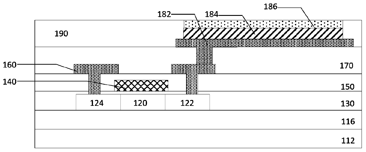
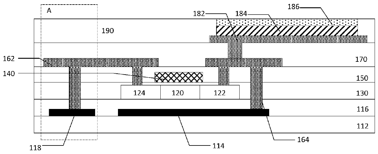
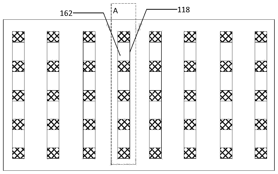
[0034] First, the prior art is briefly described. see figure 1 , figure 1 It is a schematic cross-sectional view of a display panel in the prior art. The display panel includes: a substrate 112, a thin film transistor layer and a light emitting structure.
[0035] The thin film transistor layer is located on the substrate 112 and includes a plurality of thin film t...
PUM
 Abstract
Description
Claims
Application Information