Quantum dot, preparation method thereof, quantum dot light-emitting device and related devices

A quantum dot light-emitting, quantum dot technology, applied in the fields of electric solid device, semiconductor device, semiconductor/solid state device manufacturing, etc., can solve the imbalance of electron hole injection, the effect of QLED device efficiency and life, and increase the complexity of the manufacturing process. Process uncontrollable degree and other problems, to achieve the effect of promoting injection balance, improving efficiency and life, simplifying device structure and process

Pending Publication Date: 2019-08-02
BOE TECH GRP CO LTD
View PDF6 Cites 6 Cited by
  • Summary
  • Abstract
  • Description
  • Claims
  • Application Information

AI Technical Summary

Problems solved by technology

At present, the introduction of electron transport layer material ZnO makes electron transport more efficient, so that electrons become many in QLED devices. However, due to the deep valence band of quantum dots, hole transport materials usually cannot guarantee sufficient hole injection. This leads to an imbalance in the injection of electrons and holes, which affects the efficiency and life of the QLED device. Therefore, the QLED device also needs to be provided with an electron blocking layer.
[0004] However, the preparation of the above-mentioned more functional layers increases the complexity of the manufacturing process and the degree of uncontrollability in the preparation process.

Method used


Image

  • Quantum dot, preparation method thereof, quantum dot light-emitting device and related devices
  • Quantum dot, preparation method thereof, quantum dot light-emitting device and related devices
  • Quantum dot, preparation method thereof, quantum dot light-emitting device and related devices

Examples


preparation example Construction

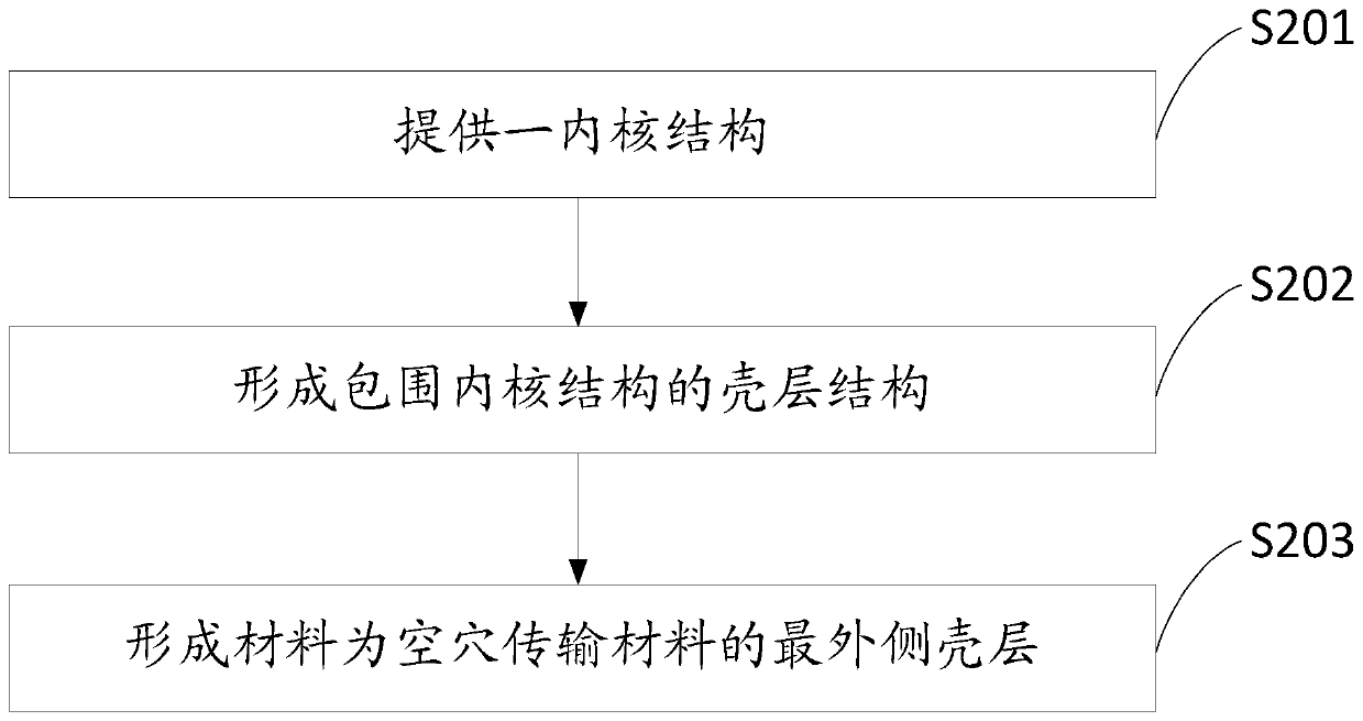
[0055] Based on the same inventive concept, the embodiment of the present invention also provides a method for preparing the above-mentioned quantum dots provided by the embodiment of the present invention, such as figure 2 shown, including:

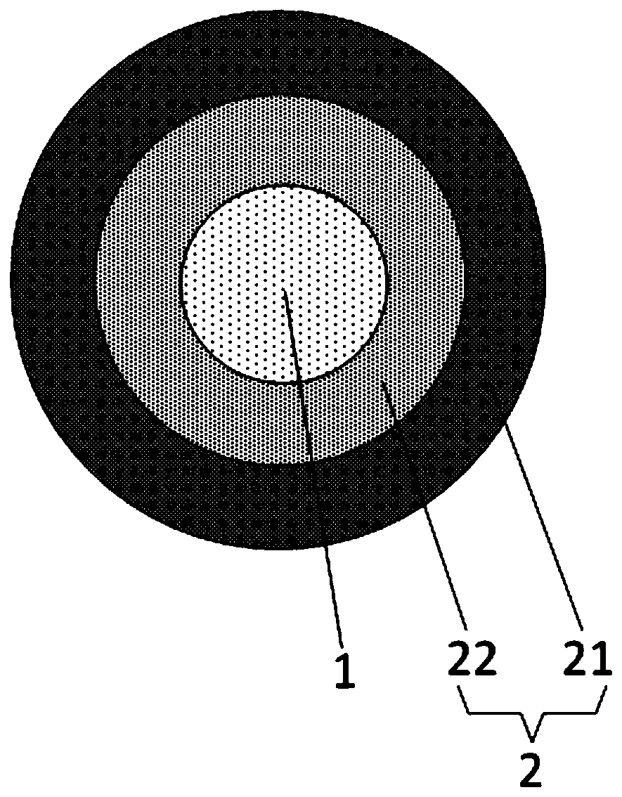
[0056] S201. Provide a kernel structure;

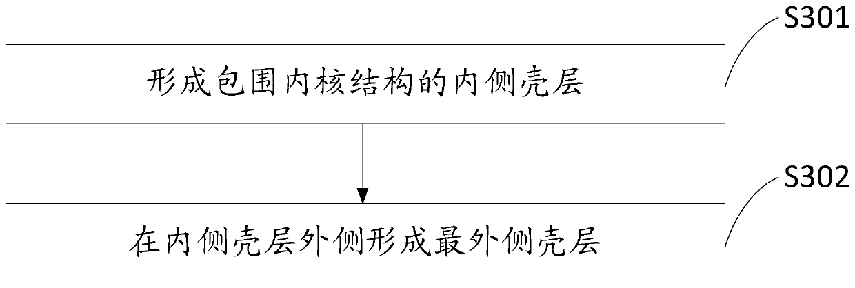
[0057] S202, forming a shell structure surrounding the core structure;

[0058] S203, forming the outermost shell layer whose material is a hole transport material.

[0059] In the preparation method of the above-mentioned quantum dots provided in the embodiment of the present invention, the outermost shell layer of the quantum dots prepared by the above-mentioned preparation method is a hole transport material, so that the quantum dots with this structure can be applied to the preparation of QLED devices. On the one hand, the outermost hole transport material of the quantum dots can be used as the hole transport layer in the QLED device, reducing the process of making a separate hole transpo...


PUM

PropertyMeasurementUnit
Thicknessaaaaaaaaaa

Abstract

The invention discloses a quantum dot, a preparation method thereof, a quantum dot light-emitting device and related devices. The outermost shell layer of the quantum dot provided by the invention isa hole transport material, so that the quantum dot with the structure can be applied to the preparation of a QLED (Quantum dot Light-Emitting Diode) device. On the one hand, the hole transport material on the outermost layer of the quantum dot can serve as a hole transport layer in the QLED device, thereby reducing the process of independently manufacturing the hole transport layer, and effectively simplifying the device structure and the technological process; and on the other hand, the hole transport material on the outermost layer of the quantum dot is contacted with an electron transport layer in the QLED device to serve as an electron blocking layer, thereby being capable of blocking part of the electron transmission. The quantum dot disclosed by the invention solves a problem that electrons are enabled to become majority carriers in the QLED device due to more efficient electron transport in the prior art, thereby effectively promoting the electron-hole injection balance, and improving the efficiency and life of the QLED device.

Description

technical field [0001] The invention relates to the field of display technology, in particular to a quantum dot and a preparation method thereof, a quantum dot light-emitting device, and a related device. Background technique [0002] Quantum dots (Quantum dots, QDs), also known as semiconductor nanocrystals and semiconductor nanoparticles, refer to nano-solid materials whose size is on the order of nanometers in three dimensions of space or composed of them as basic units. A collection of atoms and molecules. A light-emitting diode based on quantum dot materials is called a quantum dot light-emitting diode (QLED), which is a new type of light-emitting device. [0003] In a QLED device, each functional layer includes a hole injection layer, a hole transport layer, a quantum dot light-emitting layer, and an electron transport layer. Selecting a suitable device structure and matching the transfer characteristics of each functional layer are crucial to the performance of QLED...

Claims


Application Information

Patent Timeline
IPC IPC(8): H01L51/50H01L51/56
CPCH10K50/115H10K50/18H10K50/15H10K71/00
Inventor 冯靖雯
Owner BOE TECH GRP CO LTD
Why Eureka
Try Eureka