AIE (aggregation-induced emission) material-based fluorescent/phosphorescent mixed type white-light OLED and preparation method of fluorescent/phosphorescent mixed type white-light OLED
A hybrid, phosphorescence technology, applied in semiconductor/solid-state device manufacturing, electrical components, electric solid-state devices, etc., can solve problems such as low fluorescence quantum efficiency, device exciton quenching, and increased process difficulty, achieving broad application value, Simplified device structure and process, good spectral stability
- Summary
- Abstract
- Description
- Claims
- Application Information
AI Technical Summary
Problems solved by technology
Method used
Image
Examples
Embodiment 1
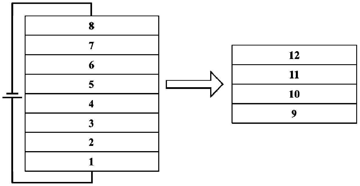
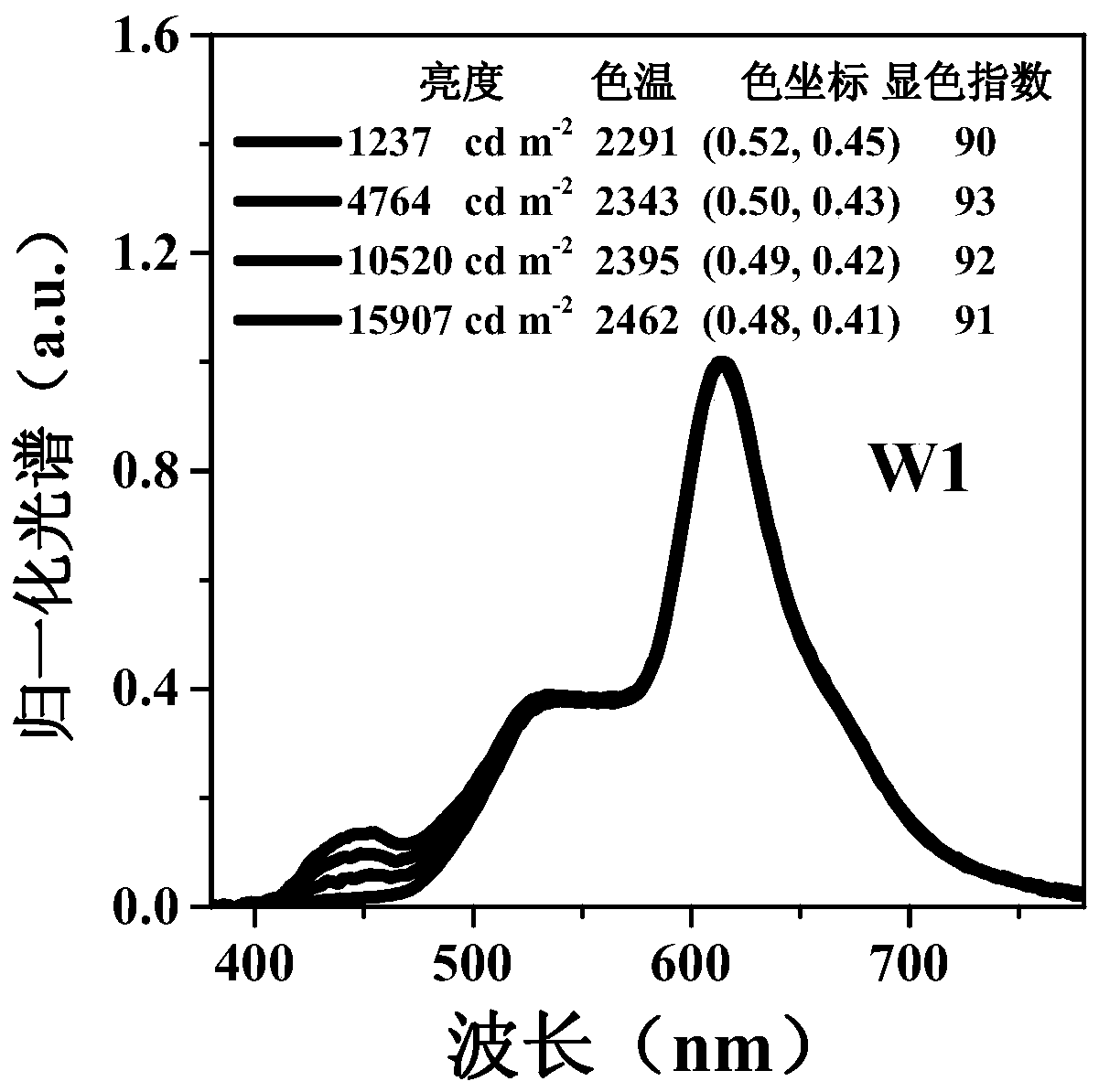
[0034] A fluorescent / phosphorescent hybrid white light OLEDs (device W1) based on aggregation-induced light-emitting materials in this embodiment uses ITO as the anode, HAT-CN as the hole injection layer, TAPC as the hole transport layer, and TCTA as the electron blocking layer , using Ir(dmdppr-mp) 2 (divm) guest-doped TCTA host is a red light-emitting layer (guest doping concentration is 3% mass percent), CP-BP-PXZ is a green light-emitting layer, TCTA is a spacer layer, TPB-AC is a blue light-emitting layer, TmPyPB It is electron transport layer, LiF is electron injection layer, and metal Al is cathode. The device structure is as follows:
[0035] Device W1: ITO / HAT-CN(5nm) / TAPC(50nm) / TCTA(5nm) / TCTA:3wt%Ir(dmppr-mp) 2 (divm)(8nm) / CP-BP-PXZ(6nm) / TCTA(2nm) / TPB-AC(10nm) / TmPyPB(40nm) / LiF(1nm) / Al(120nm).
[0036] The preparation steps of device W1 are as follows:
[0037] (1) Ultrasonic cleaning of ITO glass with cleaning agent for 60 minutes, then ultrasonic cleaning of ITO...
Embodiment 2
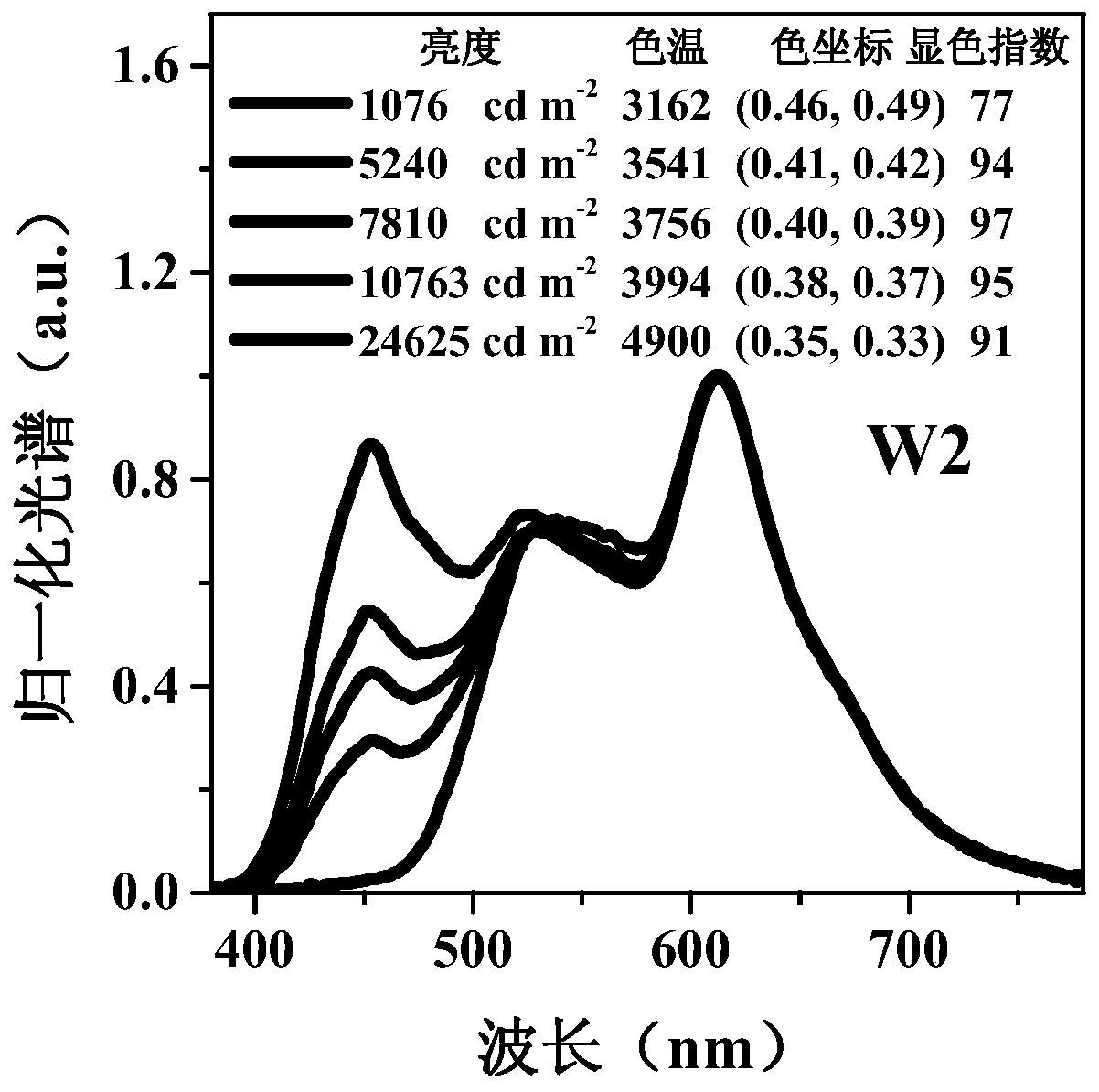
[0053] A fluorescent / phosphorescent hybrid white light OLEDs (device W2) based on aggregation-induced light-emitting materials in this embodiment differs from Example 1 only in the thicknesses of the red light-emitting layer, the spacer layer and the green light-emitting layer, and the device structure as follows:
[0054] Device W2: ITO / HAT-CN(5nm) / TAPC(50nm) / TCTA(5nm) / TCTA:3wt%Ir(dmppr-mp) 2 (divm)(5nm) / CP-BP-PXZ(10nm) / TCTA(3nm) / TPB-AC(10nm) / TmPyPB(40nm) / LiF(1nm) / Al(120nm).
[0055] The electroluminescence spectra of the white light device W2 prepared in this example at different brightnesses are as follows: image 3 As shown, its current density-brightness-voltage characteristic curve is as follows Figure 4 As shown, its power efficiency-quantum efficiency-brightness characteristic curve is as follows Figure 5 shown.
[0056] The electroluminescence performance data of the white light devices W1 and W2 prepared in the above Examples 1 and 2 are shown in Table 1:
[0...
PUM
| Property | Measurement | Unit |
|---|---|---|
| Thickness | aaaaa | aaaaa |
| Thickness | aaaaa | aaaaa |
| Thickness | aaaaa | aaaaa |
Abstract
Description
Claims
Application Information


