Inverted bottom-emitting organic light-emitting diode and preparation method thereof
A technology of light-emitting diodes and bottom emission, which is applied in the direction of organic semiconductor devices, semiconductor/solid-state device manufacturing, electrical components, etc. It can solve problems such as difficult operation and difficult evaporation, and achieve the effect of simplifying the device structure and process
- Summary
- Abstract
- Description
- Claims
- Application Information
AI Technical Summary
Problems solved by technology
Method used
Image
Examples
Embodiment 1
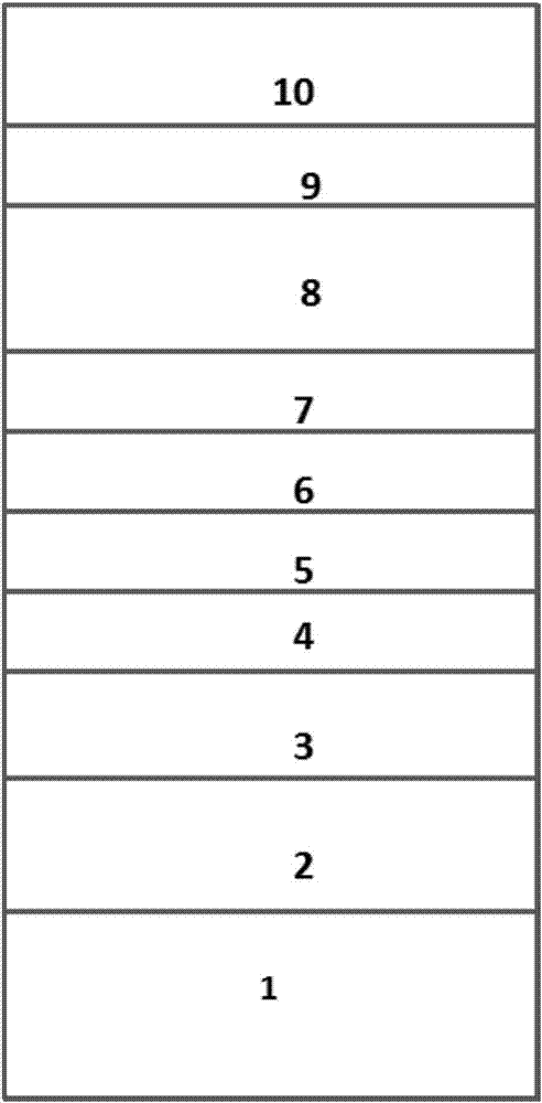
[0037] An inverted bottom-emitting organic light-emitting diode of this embodiment, its structural schematic diagram is as follows figure 1 Shown, its preparation method is as follows:
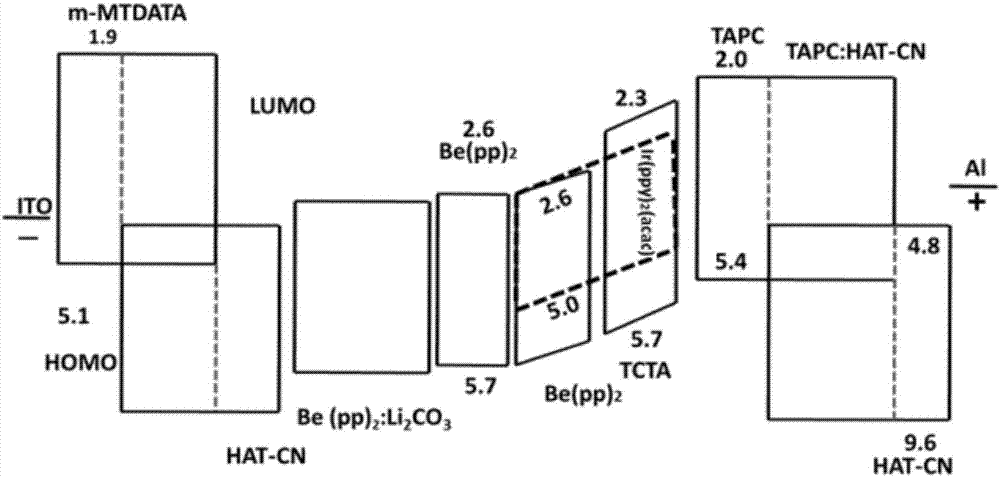
[0038] First, the ITO cathode 2 on the glass substrate 1 is photolithographically formed into an electrode with a width of 4 mm and a length of 30 mm, then cleaned, dried with nitrogen, and placed in a vacuum oven for 30 minutes at 120 degrees Celsius, and then transferred to a vacuum coating system middle. When the vacuum of the vacuum coating system reaches 1~5×10 -4 Pa, sequentially vapor-deposit m-MTDATA / m-MTDATA:HAT-CN / HAT-CN organic heterojunction charge generation layer 3, Be(pp) on the ITO cathode 2 2 : Li 2 CO 3 The electron transport layer 4, Be(pp) 2 Hole / exciton blocking layer 5, green phosphorescent dye Ir(ppy) 2 (acac) doped in the electron transport material Be(pp) respectively 2 And the double light-emitting layer 6 of the hole transport material TCTA, the electron / excit...
Embodiment 2
[0041] An inverted bottom-emitting organic light-emitting diode of this embodiment, its structural schematic diagram is as follows figure 1 Shown, its preparation method is as follows:
[0042] First, the ITO cathode 2 on the glass substrate 1 is photoetched into an electrode with a width of 4 mm and a length of 30 mm, then cleaned, dried with nitrogen, and placed in a vacuum oven for 30 minutes at 120 degrees Celsius, and then transferred to vacuum coating system. When the vacuum of the vacuum coating system reaches 1~5×10 -4 Pa, sequentially vapor-deposit m-MTDATA / m-MTDATA:HAT-CN / HAT-CN organic heterojunction charge generation layer 3, Be(pp) on the ITO cathode 2 2 : Li 2 CO 3 Electron transport layer 4, Be(pp) 2 The hole / exciton blocking layer 5, the red phosphorescent dye Ir(MDQ) 2 (acac) doped in the electron transport material NPB light-emitting layer 6, TAPC electron / exciton blocking layer 7, HAT-CN doped in the hole transport material TAPC hole transport layer 8,...
Embodiment 3
[0045] An inverted bottom-emitting organic light-emitting diode of this embodiment, its structural schematic diagram is as follows figure 1 Shown, its preparation method is as follows:
[0046] First, the ITO cathode 2 on the glass substrate 1 is photoetched into an electrode with a width of 4 mm and a length of 30 mm, then cleaned, dried with nitrogen, and placed in a vacuum oven for 30 minutes at 120 degrees Celsius, and then transferred to vacuum coating system. When the vacuum of the vacuum coating system reaches 1~5×10 -4 Pa, on the ITO cathode 2 sequentially vapor-deposited m-MTDATA / m-MTDATA:HAT-CN / HAT-CN organic heterojunction charge generation layer 3, BmPyPB:Li 2 CO 3 The electron transport layer 4 of BmPyPB, the hole / exciton blocking layer 5 of BmPyPB, and the blue phosphorescent dye FIrpic are respectively doped in the bipolar transport material 26DCzPPy and the hole transport material TCTA double light-emitting layer 6, TAPC electron / exciton blocking layer 7, H...
PUM
| Property | Measurement | Unit |
|---|---|---|
| Thickness | aaaaa | aaaaa |
| Thickness | aaaaa | aaaaa |
| Thickness | aaaaa | aaaaa |
Abstract
Description
Claims
Application Information


