Image sensor and forming method thereof

An image sensor and pixel area technology, which is applied to electric solid-state devices, semiconductor devices, electrical components, etc., can solve the problems of poor imaging quality and optical crosstalk of image sensors, and achieve the effect of preventing optical crosstalk, increasing area, and improving imaging quality.

Active Publication Date: 2019-08-09
淮安西德工业设计有限公司
View PDF6 Cites 0 Cited by
  • Summary
  • Abstract
  • Description
  • Claims
  • Application Information

AI Technical Summary

Problems solved by technology

[0004] However, if the incident angle of the incident light above the photosensitive area is too large, photons will directly enter the adjacent pixel area, resulting in optical crosstalk, resulting in poor imaging quality of the image sensor

Method used


Image

  • Image sensor and forming method thereof
  • Image sensor and forming method thereof
  • Image sensor and forming method thereof

Examples


Embodiment Construction

[0032] As mentioned in the background, the imaging quality of the image sensor is relatively poor, which will now be described in detail with reference to specific embodiments.

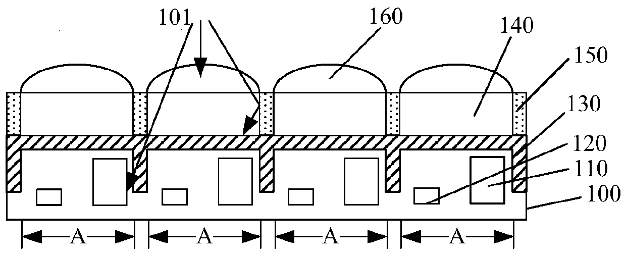
[0033] figure 1 It is a structural schematic diagram of an embodiment of an image sensor.

[0034] Please refer to figure 1 , a substrate 100, the substrate 100 includes several mutually separated pixel regions A, and an isolation region between adjacent pixel regions A; a photoelectric doped region 110 and a floating diffusion region 120 located in the pixel region A of the substrate 100; The isolation structure 130 located on the surface of the isolation area of ​​the substrate 100 and the pixel area A; the filter layer 140 located on the surface of the isolation structure 130 in the pixel area A; the reflective structure 150 located between adjacent filter layers 140; located on the surface of the filter layer 150 The microlens 160.

[0035] In the above image sensor, the reflective structure 15...


PUM


Abstract

The invention relates to an image sensor and a forming method thereof, and the image sensor comprises a first substrate, wherein the first substrate comprises a first surface and a second surface which are opposite to each other, the first substrate comprises a plurality of pixel regions which are separated from each other, and an isolation region located between adjacent pixel regions; a first reflecting structure which is located on the surface of the second surface of the first substrate; a second reflection structure which is located in the isolation region, wherein the second reflection structure penetrates from the first surface to the second surface; a second substrate which is located on the surface of the first reflection structure, wherein the second substrate comprises a third surface and a fourth surface which are opposite to each other, and the third surface is in contact with the surface of the first reflection structure, and a plurality of floating diffusion regions which are separated from one another are arranged in the second substrate; and a conductive plug which is located in the second substrate, penetrates into the second substrate from the pixel region, and is electrically connected with the floating diffusion region and the pixel region. The imaging quality of the image sensor is good.

Description

technical field [0001] The invention relates to the technical fields of semiconductor manufacturing and photoelectric imaging, in particular to an image sensor and a forming method thereof. Background technique [0002] Image sensors are classified into complementary metal oxide image sensors (CMOS Image Sensor, CIS) and charge coupled device (Charge Coupled Device, CCD) image sensors, which are usually used to convert optical signals into corresponding electrical signals. The CCD image sensor has the advantages of high image sensitivity and low noise, but it is difficult to integrate the CCD image sensor with other devices, and the CCD image sensor consumes a lot of power. In contrast, CIS has the advantages of simple process, easy integration with other devices, small size, light weight, low power consumption, and low cost. At present, CIS has been widely used in still digital cameras, camera phones, digital video cameras, medical imaging devices (such as gastroscopes), a...

Claims


Application Information

Patent Timeline
Patent Type & Authority Applications(China)
IPC IPC(8): H01L27/146
CPCH01L27/14601H01L27/14603H01L27/14629H01L27/1463H01L27/14643H01L27/14685H01L27/14689
Inventor 吴明吴孝哲林宗贤吴龙江熊建锋朱晓彤
Owner 淮安西德工业设计有限公司
Why Eureka
Try Eureka