

Display substrate and manufacturing method thereof
A technology for display substrates and substrates, used in semiconductor/solid-state device manufacturing, instruments, electrical components, etc.
- Summary
- Abstract
- Description
- Claims
- Application Information
AI Technical Summary
Problems solved by technology
Method used
Image

Examples
no. 1 example
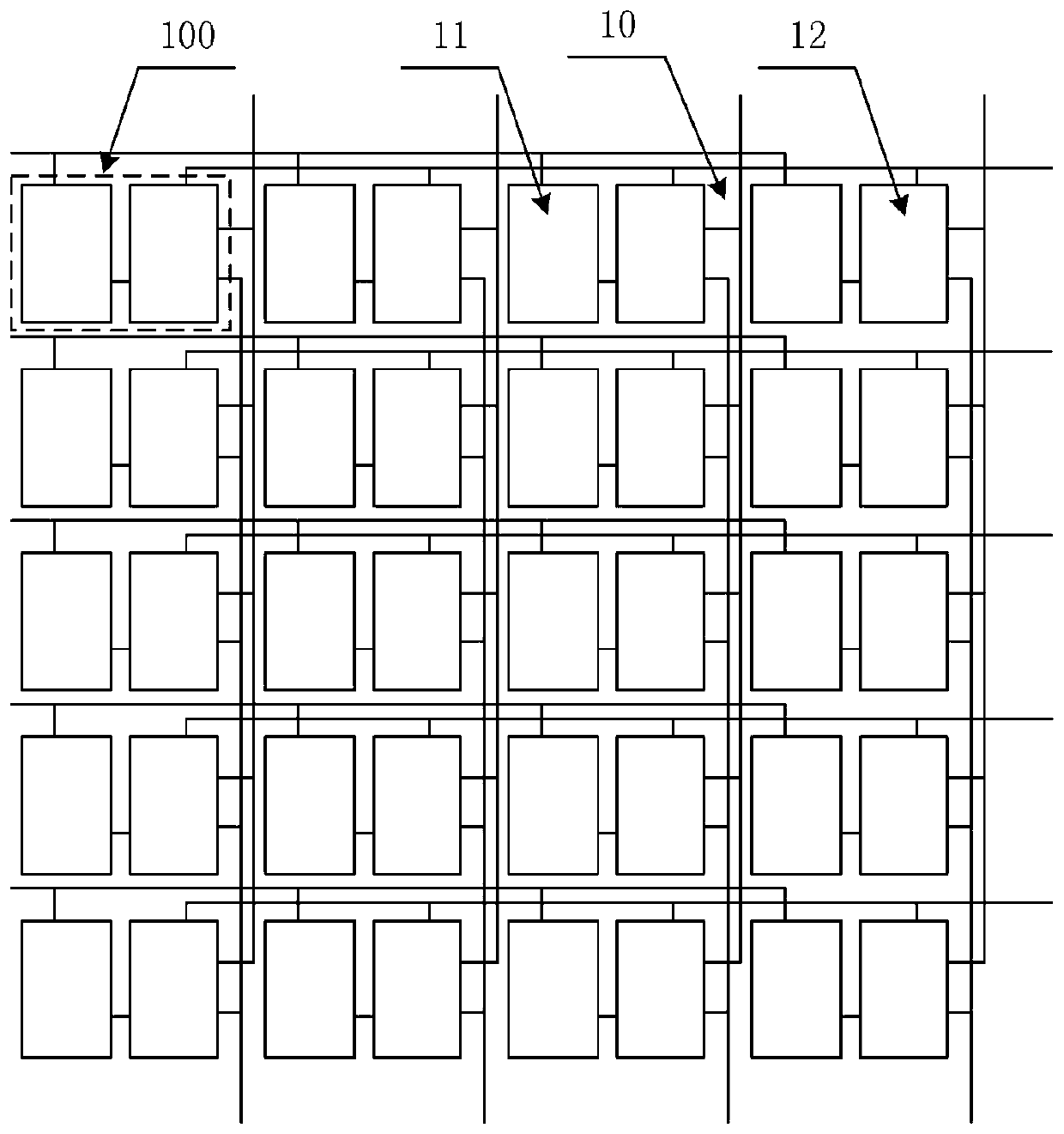
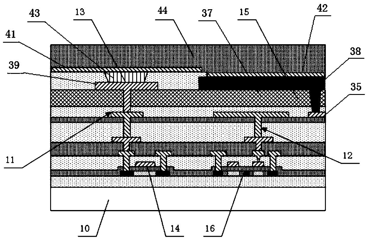
[0069] The display substrate of this embodiment is prepared by a complementary metal-oxide-semiconductor (Complementary MetalOxide Semiconductor, CMOS) process. Such as figure 2 As shown, the embodiment of the present invention shows that the display substrate includes a base 10, and a light emitting structure layer 11 and a fingerprint recognition structure layer 12 formed on the base 10. The light emitting structure layer 11 includes a light emitting unit 13 and a light emitting driving circuit 14. The light emitting unit 13 is used for The display light is emitted, and the light-emitting drive circuit 14 is used to control and drive the light-emitting unit 13 . The fingerprint identification structure layer 12 includes a fingerprint identification sensor 15 and a processing circuit 16. The fingerprint identification sensor 15 is used to form a fingerprint electrical signal, and the processing circuit 16 is used to receive the fingerprint electrical signal from the fingerpr...
no. 2 example
[0095] Figure 13 A schematic diagram showing the structure of the second embodiment of the substrate according to the present invention shows a structure prepared by using an N-channel metal-oxide-semiconductor (Negative Channel Metal Oxide Semiconductor, NMOS) process.
[0096] Such as Figure 13 As shown, the display substrate of this embodiment includes a base 10 , and a light emitting structure layer 11 and a fingerprint recognition structure layer 12 formed on the base 10 . The light-emitting structure layer 11 includes a light-emitting unit and a light-emitting drive circuit. The fingerprint recognition structure layer 12 includes a fingerprint recognition sensor for forming fingerprint electrical signals. The fingerprint recognition sensor includes a piezoelectric film layer, and the piezoelectric film layer is located between the light-emitting unit and the light-emitting drive circuit. and cover the pixel unit, the light emitting unit penetrates through the piezoele...
no. 3 example
[0100] Figure 14 A schematic diagram showing the structure of the third embodiment of the substrate according to the present invention shows a structure prepared by using a P-channel metal-oxide-semiconductor (Positive Channel Metal Oxide Semiconductor, PMOS) process.
[0101] Such as Figure 14 As shown, the display substrate of this embodiment includes a base 10 , and a light emitting structure layer 11 and a fingerprint recognition structure layer 12 on the base 10 . The light-emitting structure layer 11 includes a light-emitting unit and a light-emitting drive circuit. The fingerprint recognition structure layer 12 includes a fingerprint recognition sensor for forming fingerprint electrical signals. The fingerprint recognition sensor includes a piezoelectric film layer, and the piezoelectric film layer is located between the light-emitting unit and the light-emitting drive circuit. and cover the pixel unit, the light emitting unit penetrates through the piezoelectric thi...
PUM
 Abstract
Description
Claims
Application Information