

Touch control and fingerprint identification module, manufacture method thereof, and electronic terminal
A fingerprint recognition module and fingerprint recognition technology, applied in the field of human-computer interaction, can solve the problem of occupying mobile phone space, and achieve the effects of cost saving, convenient operation, and effective use of screen space
- Summary
- Abstract
- Description
- Claims
- Application Information
AI Technical Summary
Problems solved by technology
Method used
Image

Examples
Embodiment 1
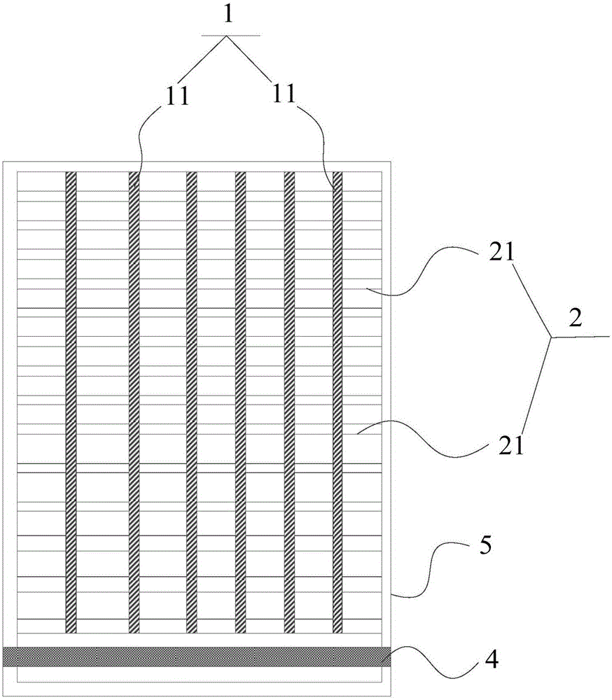
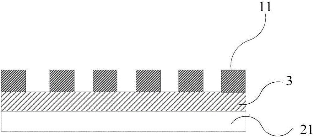
[0106] combine figure 1 and figure 2 , a touch and fingerprint recognition module, including: a first electrode layer 1 as a receiving electrode, a second electrode layer 2 as an emitter, and a spacer layer between the first electrode layer 1 and the second electrode layer 2 The insulating layer 3; the first electrode layer 1, used as the first electrode layer for fingerprint recognition and touch control, includes a plurality of first electrode lines 11 arranged in sequence. The second electrode layer 2, as the second electrode layer for fingerprint identification and touch control, includes a plurality of second electrode lines 21 arranged in sequence; the first electrode lines 11 of the first electrode layer 1 and the second electrode lines of the second electrode layer 2 The electrode lines 21 are arranged in a staggered manner. The first electrode lines 11 and the second electrode lines 21 are made of ITO material. The insulating layer 3 is made of insulating resin. ...
Embodiment 2
[0109] Implementation 1 was repeated, except that the line width of the first electrode lines 11 was 0.01 mm; the line width of the second electrode lines 21 was 0.01 mm. The distance between two adjacent first electrode lines 11 is 0.15 mm; the distance between two adjacent second electrode lines 21 is 0.15 mm. The first electrode lines 11 and the second electrode lines 21 form an angle of 90° with each other, that is, they are perpendicular.
[0110] Taking 5 inches as an example, the size of the viewing area is 62.1mm*110.4mm, the distance between the receiving electrode and the emitting electrode is 0.15*0.15mm, and the width of a single metal wire is 0.01mm. (414) + emitter (736), the sum of the two requires a total of 1150 PADs (pins), and the metal lead is pulled down to the bottom of the glass to connect the processing chip.
Embodiment 3
[0112] Embodiment 1 was repeated, except that the line width of the first electrode lines 11 was 0.005 mm; the line width of the second electrode lines 21 was 0.002 mm. The distance between two adjacent first electrode lines 11 is 0.08 mm; the distance between two adjacent second electrode lines 21 is 0.06 mm. The first electrode lines 11 and the second electrode lines 21 form an angle of 90° with each other, that is, they are perpendicular.
[0113] Taking 5 inches as an example, the size of the visible area is 62.1mm*110.4mm, the distance between the receiving electrode and the emitter electrode is 0.08*0.06mm, the width of a single first electrode metal wire is 0.05mm, and the width of a single second electrode The width of the electrode metal wire is 0.002mm, and the visible area requires a total of receiving electrodes (776) + emitters (1833). The sum of the two requires a total of 2609 PADs (pins). Pull the metal leads down to the bottom of the glass and connect the proc...
PUM
 Abstract
Description
Claims
Application Information