Array substrate, display panel and display device

A technology for array substrates and base substrates, which is applied in the fields of array substrates, display panels and display devices, and can solve problems such as poor high temperature resistance of quantum dot materials

Active Publication Date: 2021-09-21
BOE TECH GRP CO LTD
View PDF9 Cites 0 Cited by
  • Summary
  • Abstract
  • Description
  • Claims
  • Application Information

AI Technical Summary

Problems solved by technology

However, due to the poor high temperature resistance of quantum dot materials, there is a compatibility problem in the normal array process

Method used


Image

  • Array substrate, display panel and display device
  • Array substrate, display panel and display device
  • Array substrate, display panel and display device

Examples


Embodiment Construction

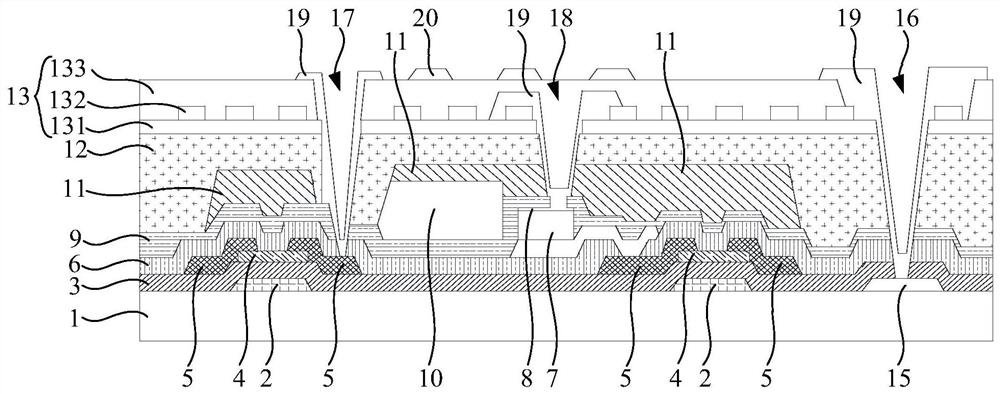
[0030] The following will clearly and completely describe the technical solutions in the embodiments of the present invention with reference to the accompanying drawings in the embodiments of the present invention. Obviously, the described embodiments are only some, not all, embodiments of the present invention. Based on the embodiments of the present invention, all other embodiments obtained by persons of ordinary skill in the art without making creative efforts belong to the protection scope of the present invention.

[0031] Please refer to figure 1 , the present invention provides an array substrate, comprising:

[0032] substrate substrate 1;

[0033] A patterned thin film transistor layer disposed on the base substrate 1;

[0034] The first passivation layer 9 disposed on the side of the thin film transistor layer away from the base substrate 1;

[0035] A quantum dot layer 10 disposed on the side of the first passivation layer 9 away from the base substrate 1 and loc...


PUM


Abstract

The present invention relates to the technical field of display devices, and discloses an array substrate, a display panel and a display device. The array substrate includes: a base substrate; a patterned thin film transistor layer and a first passivation layer sequentially arranged on the base substrate , a quantum dot layer, a color filter layer, a flat layer and a metal wire grid polarizing layer, wherein the orthographic projection of the quantum dot layer on the substrate is located within the orthographic projection of the color filter layer on the substrate. In the array substrate, both the quantum dot layer and the metal wire grid polarizing layer are arranged on the base substrate, and the thermal influence on the quantum dot layer in the manufacturing process is blocked by the color filter layer, and the backlight is improved by wavelength conversion. Utilization, thus meeting the display requirements.

Description

technical field [0001] The present invention relates to the technical field of display devices, in particular to an array substrate, a display panel and a display device. Background technique [0002] With the development of liquid crystal display products, the transmittance and color gamut of liquid crystal panels have been limited by bottlenecks, and wavelength conversion has to be used to improve the utilization rate of backlight to meet display requirements. [0003] The quantum dot material is an excellent wavelength conversion material. The quantum dot material is made into a photoresist to form a quantum dot film layer with a pixel-level pattern, which can specifically convert the backlight into the color required by the pixel, and greatly improve the backlight utilization. Rate. However, due to the fluorescent properties of quantum dot materials, it will completely destroy the polarization state of light, so it must be used with a built-in polarizer. At present, th...

Claims


Application Information

Patent Timeline
Patent Type & Authority Patents(China)
IPC IPC(8): H01L27/12
CPCH01L27/1214H01L27/1259G02F1/133548G02F1/133614G02F1/133617G02F2202/36G02F1/13318G02F1/136222G02F1/136209G02F1/1368
Inventor 舒适李翔徐传祥于勇黄海涛岳阳姚琪黄睿石戈郭康
Owner BOE TECH GRP CO LTD
Why Eureka
Try Eureka