Heterojunction solar cell with plated seed layer prepared by in-situ reduction, and preparation method thereof

A technology of solar cells and seed layers, which is applied in circuits, photovoltaic power generation, electrical components, etc., can solve the problems of complex processes and many consumables, and achieve the effects of good uniformity, reduced interface contact resistance, and reduced process complexity

Inactive Publication Date: 2019-08-16
SOUTHWEST PETROLEUM UNIV
View PDF6 Cites 6 Cited by
  • Summary
  • Abstract
  • Description
  • Claims
  • Application Information

AI Technical Summary

Problems solved by technology

[0007] The most commonly used methods for preparing metal seed layers at present: physical vapor deposition (including PVD, sputtering, etc.), chemical vapor deposition, inkjet printing, printing, spraying, electroplating, electroless plating, etc., but the above-mentioned traditional methods for forming seed layers The process is relatively complicated and there are many consumables. The present invention starts from the direction of improving the contact characteristics between the transparent conductive film and the metal electrode, simplifying the process, and lowering the cost, and realizes the process of using the electrochemical reduction method to prepare the metal seed layer. has obvious advantages in

Method used


Image

  • Heterojunction solar cell with plated seed layer prepared by in-situ reduction, and preparation method thereof
  • Heterojunction solar cell with plated seed layer prepared by in-situ reduction, and preparation method thereof
  • Heterojunction solar cell with plated seed layer prepared by in-situ reduction, and preparation method thereof

Examples


Embodiment Construction

[0046] The present invention will be further described below in conjunction with the embodiments and the accompanying drawings.

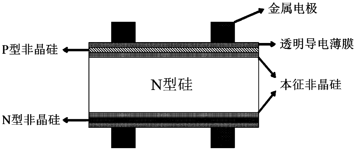
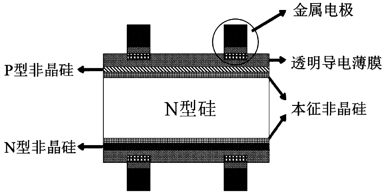
[0047] Such as image 3 and 4 As shown, a heterojunction solar cell for preparing an electroplating seed layer by in-situ reduction of the present invention has the following structure:

[0048] Cu / Ni / In / ITO / p-a-Si / i-a-Si / n-c-Si / i-a-Si / n-a-Si / ITO / In / Ni / Cu, where Cu is metal copper, Ni is metal nickel, and In is metal Indium, ITO is tin-doped indium oxide transparent conductive film, p-a-Si is P-type amorphous silicon film, i-a-Si is intrinsic amorphous silicon film, n-c-Si is N-type single crystal silicon substrate, n-a-Si It is an N-type amorphous silicon film.

[0049] The preparation process of this embodiment is as follows Figure 6 Shown:

[0050] (1) Perform damage removal and surface texturing on the N-type single crystal silicon substrate layer;

[0051] (2) Depositing an intrinsic amorphous silicon film on both side surfaces of the N-...


PUM

PropertyMeasurementUnit
thicknessaaaaaaaaaa
thicknessaaaaaaaaaa
thicknessaaaaaaaaaa

Abstract

The invention discloses a heterojunction solar cell with a plated seed layer prepared by in-situ reduction, and a preparation method thereof. The heterojunction solar cell comprises an N-type monocrystalline silicon substrate layer; an intrinsic amorphous silicon film; a P-type amorphous silicon film; an N-type amorphous silicon film; a transparent conductive film; a plated metal electrode which comprises a metal seed layer formed on the transparent conductive film by electrochemical in-situ reduction; and a metal conducting layer plated on the surface of the metal seed layer. Compared with atraditional plated electrode preparation method, the method can significantly reduce process complexity, forms a seed layer by an electrochemical method, improves interface adhesion characteristics, reduces interface contact resistance, improves the performance of the heterojunction solar cell, and achieve high efficiency and low cost.

Description

technical field [0001] The invention relates to a heterojunction solar cell for preparing an electroplating seed layer by in-situ reduction and a preparation method thereof, and belongs to the field of heterojunction solar cells. Background technique [0002] The energy crisis has aroused people's concern more and more, and environmental pollution has also produced a threat to people's lives. The more urgent problem at present is to develop some new green energy, such as solar energy, wind energy, nuclear energy, biological energy and so on. In modern society, with the rapid growth of the world's population, all countries are vigorously developing technology and economy, and no matter which aspect of development requires energy supply, human demand for it is increasing day by day. Under such a social background, the way of promoting economic development has also undergone tremendous changes, improving the level of manufacturing technology and improving the quality of life of...

Claims


Application Information

Patent Timeline
Patent Type & Authority Applications(China)
IPC IPC(8): H01L31/0224H01L31/072H01L31/18
CPCH01L31/022425H01L31/072H01L31/1804H01L31/1876Y02E10/547Y02P70/50
Inventor 俞健李君君陈涛黄跃龙
Owner SOUTHWEST PETROLEUM UNIV
Why Eureka
Try Eureka