3c Manufacturing method of curved shell for electronic device

The technology of an electronic device and manufacturing method, which is applied in the field of shell manufacturing, can solve the problems of long production time, waste of cost, difficulty in achieving smooth and wrinkle-free finished products, etc.

Active Publication Date: 2021-09-10
何英信
View PDF11 Cites 0 Cited by
  • Summary
  • Abstract
  • Description
  • Claims
  • Application Information

AI Technical Summary

Problems solved by technology

The above process is mainly to provide a first colloid between the first and second fiberglass boards, and to age the first colloid for a long time to form a buffer adhesive layer and combine it between the first and second fiberglass boards; therefore, In the process, it has the defects of long production time and waste of cost (requires two glass fiber boards)
[0005] Due to the above-mentioned defects, there is a design of directly pasting the film on the fiberglass board, but because each brand of electronic products has its own brand LOGO, and each brand has its own place to display the LOGO, so in the process of film pasting, Alignment deviations often occur due to machine modules or human problems, so that the LOGO can be placed in the correct position, resulting in yield problems; in addition, because most of the casings have curved arcs around, when in the When pasting the film, the curved edge of the casing will cause the film to wrinkle. Therefore, it is difficult to achieve a smooth and wrinkle-free finished product. This is a major subject for research and development in the industry.

Method used


Image

  • 3c Manufacturing method of curved shell for electronic device
  • 3c Manufacturing method of curved shell for electronic device
  • 3c Manufacturing method of curved shell for electronic device

Examples


Embodiment Construction

[0028] The present invention is to make use of technology content, the effectiveness of the invention and its purpose is to reach a more complete and clear expose, now at the detailed description, and please also refer to the uncovering of plans and drawings:

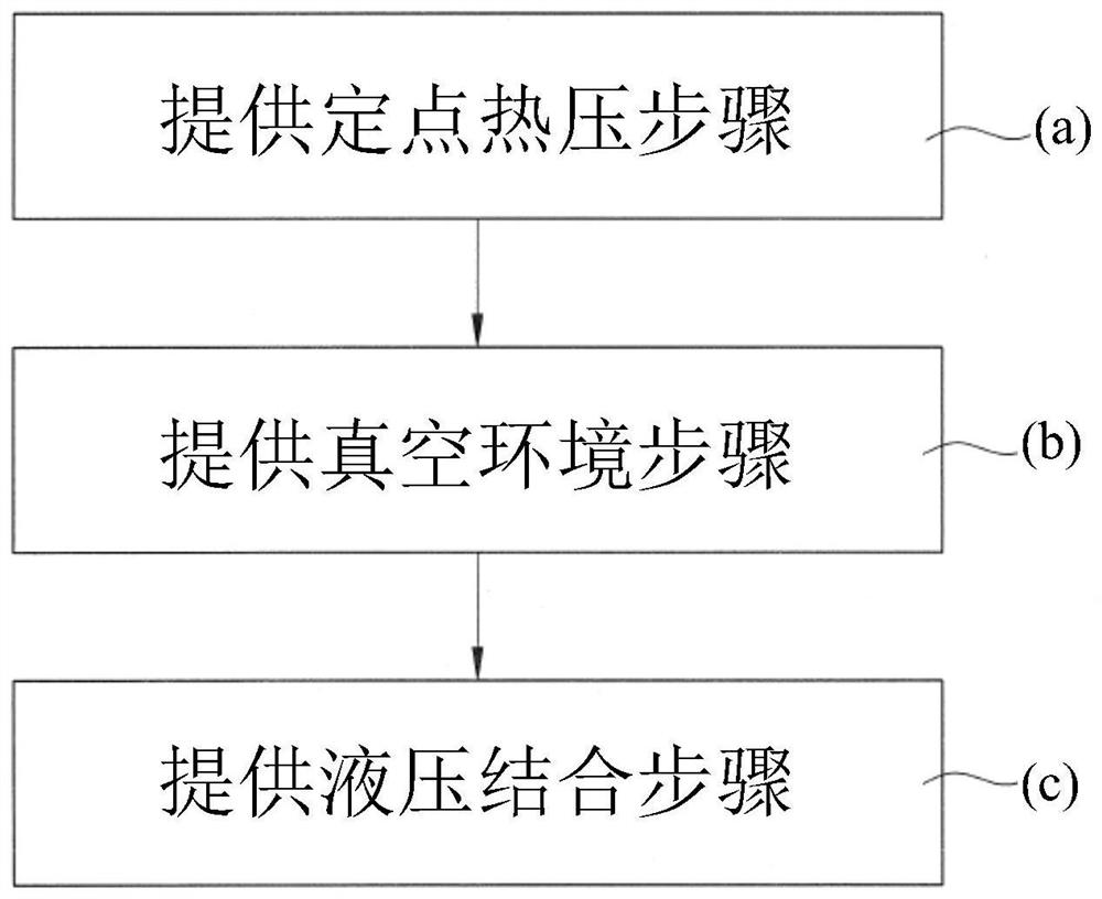
[0029] First, please see Figure 1 ~ 4 , The steps of the method of manufacturing a housing surface 3C of the electronic device of the present invention and a schematic cross-sectional view, which comprises the steps of:

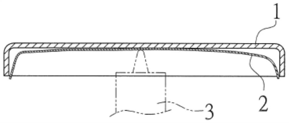
[0030] (A) providing a pointing pressing step, curved arc having a light-transmitting base shell design features a decorative film 2, using the thermal head 3 and the decorative film 2 is subjected to hot point, and positioned in the bonded the transparent substrate 1 case;

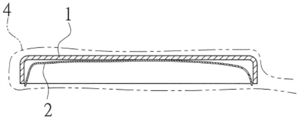
[0031] (B) the step of providing a vacuum environment, the point bonding said decorative shell of the light-transmissive film 2 is placed in a vacuum bag 4, and the vacuum is drawn, the decorative film 2 and the transparent substrate ...


PUM


Abstract

The invention relates to a method for manufacturing a curved shell of a 3C electronic device. It mainly provides a decorative film in a light-transmitting base shell with a curved arc design, and uses fixed-point hot pressing to produce a bonding position, and then places the light-transmitting base shell Put it in a vacuum-tight space, so that the decorative film can be closely attached to the transparent base shell, and then provide a hydraulic environment, so that the decorative film can be smoothly combined with the surface of the transparent base shell in a high-pressure, high-temperature liquid solvent ; By this method, the pattern in the curved shell can be accurately aligned, and can be bonded evenly under the state of equal pressure of the liquid, without wrinkling at the curved part, so as to achieve the effect of improving the manufacturing yield of the curved shell.

Description

Technical field [0001] The present invention has a housing for a method of manufacturing the surface 3C of the electronic device, especially one having a curved surface, the curved arc portion of the manufacturing method of the housing, the interior of the main housing pattern allows an accurate alignment, and are pressed in the liquid bonding the flat state, without generating wrinkles curved arc portion phenomenon invention for its application. Background technique [0002] With the progress of modern society and the development of science and technology, people have become increasingly demanding consumer electronics products (such as slim and light volume, diverse functions, textured appearance, etc.). Therefore, the current consumer electronics products to thin and light design concept based. On the current common market of high-end electronic products, its shell material is typically a metal or carbon fiber composite material based. Two materials are lightweight and has high...

Claims


Application Information

Patent Timeline
Patent Type & Authority Patents(China)
IPC IPC(8): B29C63/30B29C63/00
CPCB29C63/0073B29C63/0091B29C63/30B29C2791/006B29C2791/007
Inventor 何英信
Owner 何英信
Why Eureka
Try Eureka