OLED display panel and manufacturing method thereof

A technology for display panels and substrates, which is used in semiconductor/solid-state device manufacturing, semiconductor devices, electrical components, etc., and can solve problems such as increased risk of failure, poor stability, and film breakage.

Active Publication Date: 2019-08-27
BOE TECH GRP CO LTD +1
View PDF3 Cites 0 Cited by
  • Summary
  • Abstract
  • Description
  • Claims
  • Application Information

AI Technical Summary

Problems solved by technology

When the current hole-digging method cuts the area that needs to be opened, the cut section of the self-luminous layer in the OLED device will be exposed to the external environment, and the water vapor and oxygen in the external environment will corrode and damage the self-luminous layer, resulting in OLED device damage, such as image 3 shown, where image 3 The OLED display panel in includes a substrate 10, an OLED device 20 disposed on the substrate 10, and an encapsulation layer 30 encapsulating the OLED device 20
[0003] At present, in order to solve the problem that the cut section of the self-luminous layer in the above-mentioned OLED device is exposed to the external environment, an inverted trapezoidal structure 50 can be set in the hole-digging area, and then the holes are dug by two encapsulation methods. For the structural diagram, refer to Figure 4 , the display panel includes a substrate 10, a first encapsulation layer 31, a flat layer 40, an OLED device 20, a second encapsulation layer 32, and an inverted trapezoidal structure 50, the setting of the inverted trapezoidal structure can reduce the residue of encapsulation material during cutting, and the inverted Compared with the positive trapezoidal structure, the trapezoidal structure has poorer stability and is easy to fall off during cutting. The above method can effectively cut and form through holes, but the setting of the inverted trapezoidal structure not only increases the MASK process, but also deposits other films on the inverted trapezoidal structure. The unfavorable phenomenon of film layer breakage (under out) is prone to occur in the multi-layer structure, which increases the risk of failure. In addition, the OLED device needs to be packaged twice, which increases the complexity of the process.

Method used


Image

  • OLED display panel and manufacturing method thereof
  • OLED display panel and manufacturing method thereof
  • OLED display panel and manufacturing method thereof

Examples


Embodiment Construction

[0038] The embodiments of the present invention are described in detail below. The embodiments described below are exemplary, and are only used to explain the present invention, but should not be construed as limiting the present invention. Where specific techniques or conditions are not indicated in the embodiments, the procedures shall be carried out in accordance with the techniques or conditions described in the literature in the field or in accordance with the product specification. The reagents or instruments used without the manufacturer's indication are all conventional products that are commercially available.

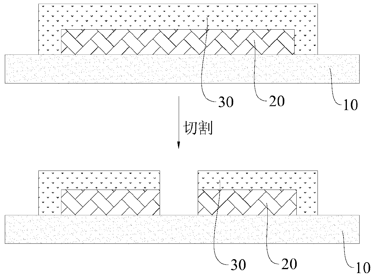
[0039] In one aspect of the present invention, the present invention provides a method of manufacturing an OLED display panel. According to an embodiment of the present invention, refer to Figure 5 , The method of making OLED display panel includes:

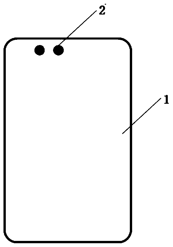
[0040] S100: A substrate 10 is provided. The substrate 10 is divided into a through hole area S. Refer to the st...


PUM


Abstract

The invention provides an OLED display panel and a manufacturing method thereof. The method for manufacturing the OLED display panel comprises the following steps that a substrate is provided, whereinthe substrate is divided into a through hole area; a hydrophilic-hydrophobic transition layer is formed in the through hole area; the surface state of the hydrophilic-hydrophobic transition layer isa in a hydrophilic state; a plurality of OLED devices are formed on the surface of the substrate, wherein a gap is formed between the orthographic projections of the plurality of OLED devices on the substrate and the orthographic projection of the through hole area on the substrate; a packaging layer is formed on the surfaces of the OLED devices, the surface of the hydrophilic-hydrophobic transition layer and the exposed surface of the substrate; the state of the hydrophilic-hydrophobic transition layer on the surface of the through hole area is changed from the hydrophilic state into the a hydrophobic state; and the hydrophilic-hydrophobic transition layer and the packaging layer are removed, wherein the orthographic projection of the hydrophilic-hydrophobic transition layer on the substrate is overlapped with the orthographic projection of the through hole area on the substrate. Therefore, the hydrophilic-hydrophobic transition layer corresponding to the through hole area and the packaging layer can be removed in a relatively easy, quick and complete mode, so that the formation of a subsequent through hole is facilitated; and the process is simple, and the adverse risk in manufacturing can be reduced.

Description

Technical field [0001] The present invention relates to the field of display technology, in particular, to an OLED display panel and a manufacturing method thereof. Background technique [0002] Organic electroluminescent devices (OLEDs) are display lighting devices that have gradually developed in recent years. Due to their advantages of high response, high contrast, flexibility, etc., they are regarded as having broad application prospects. An OLED device generally includes a substrate, a TFT structure disposed on the substrate, a self-luminous layer disposed on the TFT structure, and an encapsulation film that encapsulates the self-luminous layer. reference figure 1 As shown, when making OLED devices, it is generally necessary to make holes in the display area 1 of the OLED device to form a circular hole 2 for placing cameras, earpieces and other components, and many wearable products also need to be dug. In order to add other objects, such as figure 2 As shown, dig a hole i...

Claims


Application Information

Patent Timeline
Patent Type & Authority Applications(China)
IPC IPC(8): H01L51/56H01L51/52H01L27/32
CPCH10K59/12H10K50/8426H10K50/844H10K71/00
Inventor 徐元杰
Owner BOE TECH GRP CO LTD
Why Eureka
Try Eureka