Image sensor and manufacturing method thereof

An image sensor and photosensitive element technology, which is applied to electric solid state devices, semiconductor devices, radiation control devices, etc., to achieve the effect of increasing full well capacity, increasing lateral size, and increasing full well capacity

Inactive Publication Date: 2019-09-06
HUAIAN IMAGING DEVICE MFGR CORP
View PDF5 Cites 1 Cited by
  • Summary
  • Abstract
  • Description
  • Claims
  • Application Information

AI Technical Summary

Problems solved by technology

[0005] This application provides an image sensor and its manufacturing method for the problem that ion implantation energy limits the improvement of the full well capacity of a single pixel unit in the prior art, which can improve the full well capacity of each pixel unit in the image sensor

Method used


Image

  • Image sensor and manufacturing method thereof
  • Image sensor and manufacturing method thereof
  • Image sensor and manufacturing method thereof

Examples


Embodiment Construction

[0023] The following description provides specific application scenarios and requirements of the application, with the purpose of enabling those skilled in the art to manufacture and use the contents of the application. Various local modifications to the disclosed embodiments will be readily apparent to those skilled in the art, and the general principles defined herein may be applied to other embodiments and embodiments without departing from the spirit and scope of the disclosure. application. Thus, the present disclosure is not limited to the embodiments shown, but is to be accorded the widest scope consistent with the claims.

[0024] The technical solution of the present invention will be described in detail below in conjunction with the embodiments and the accompanying drawings.

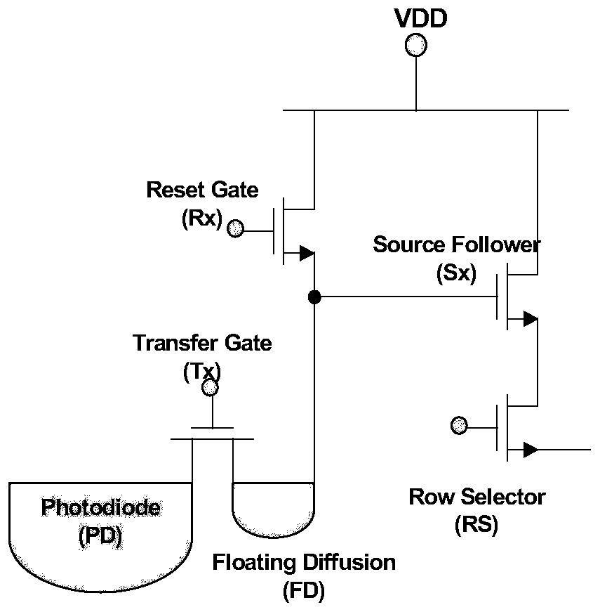
[0025] The embodiment of this application provides an image sensor, refer to the attached figure 1 Shown is a circuit diagram of a CMOS image sensor, more specifically, a circuit diagram of a...


PUM


Abstract

The invention relates to an image sensor and a manufacturing method thereof. The image sensor comprises a semiconductor substrate, an epitaxial layer located on the surface of the semiconductor substrate, a photosensitive element, wherein the photosensitive element comprises a first photosensitive element positioned in the semiconductor substrate and a second photosensitive element positioned in the epitaxial layer; and the second photosensitive element extends to the first photosensitive element. According to the image sensor, the epitaxial layer is grown on the semiconductor substrate, and the first photosensitive element and the second photosensitive element are formed on the semiconductor substrate and the epitaxial layer respectively, so that the process limitation caused by single manufacturing of the light sensing elements is avoided, and the longitudinal size of the light sensing elements is increased, the full-well capacity of each pixel unit is improved; and in addition, thetransistors of the pixel units of the image sensor are formed on the epitaxial layer, so that the transverse size of the photosensitive elements is enlarged, and the full-well capacity of each pixel unit is improved.

Description

technical field [0001] The present application relates to the field of manufacturing semiconductor devices, in particular to an image sensor and a manufacturing method thereof. Background technique [0002] An image sensor is a device that converts an optical image into an electrical signal. With the development of the computer and communication industries, the demand for high-performance image sensors is increasing. These high-performance image sensors are widely used in digital cameras, video recorders, personal communication systems (PCS), game consoles, security cameras, and medical miniature cameras. various fields. [0003] In the current field of image sensor development, the factors that determine its advantages are mainly the number of pixels and the full well capacity of each pixel. How to improve the full well capacity of a single pixel is a very worthwhile research direction. In the current solution for improving the full well capacity, the main method is to in...

Claims


Application Information

Patent Timeline
Patent Type & Authority Applications(China)
IPC IPC(8): H01L27/146
CPCH01L27/14605H01L27/1461H01L27/14612H01L27/14687
Inventor 李岩杨健李超马富林
Owner HUAIAN IMAGING DEVICE MFGR CORP
Why Eureka
Try Eureka