Coupled inductor structure

A technology of coupled structure and coupled inductance, applied in circuits, electrical components, electric solid devices, etc., can solve the problems such as the self-resonant frequency cannot be too high, the quality factor of the coupled inductance is not ideal, and the frequency of use is limited, so as to improve the utilization of chip area. rate effect

Pending Publication Date: 2018-12-18
格兰康希通信科技(上海)股份有限公司
View PDF0 Cites 0 Cited by
  • Summary
  • Abstract
  • Description
  • Claims
  • Application Information

AI Technical Summary

Problems solved by technology

The quality factor of the coupled inductance formed under the limitation of the process is not ideal, and the coupled inductance generally does not exceed 15nH, which often ca

Method used


Image

  • Coupled inductor structure
  • Coupled inductor structure
  • Coupled inductor structure

Examples


Example Embodiment

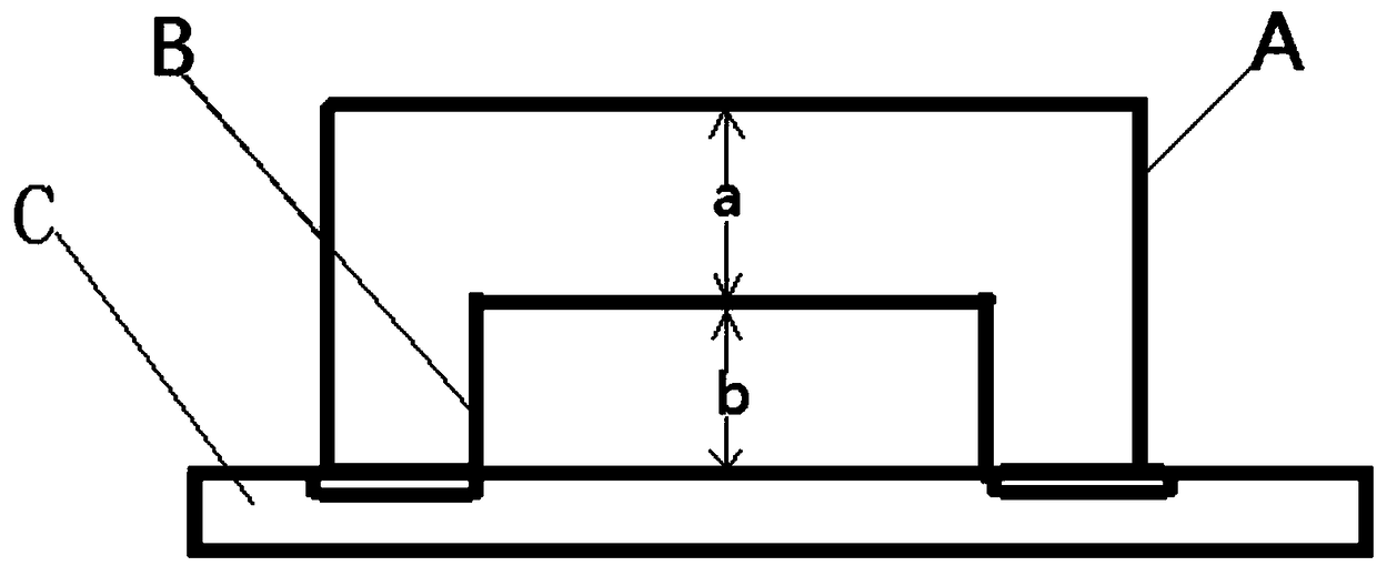
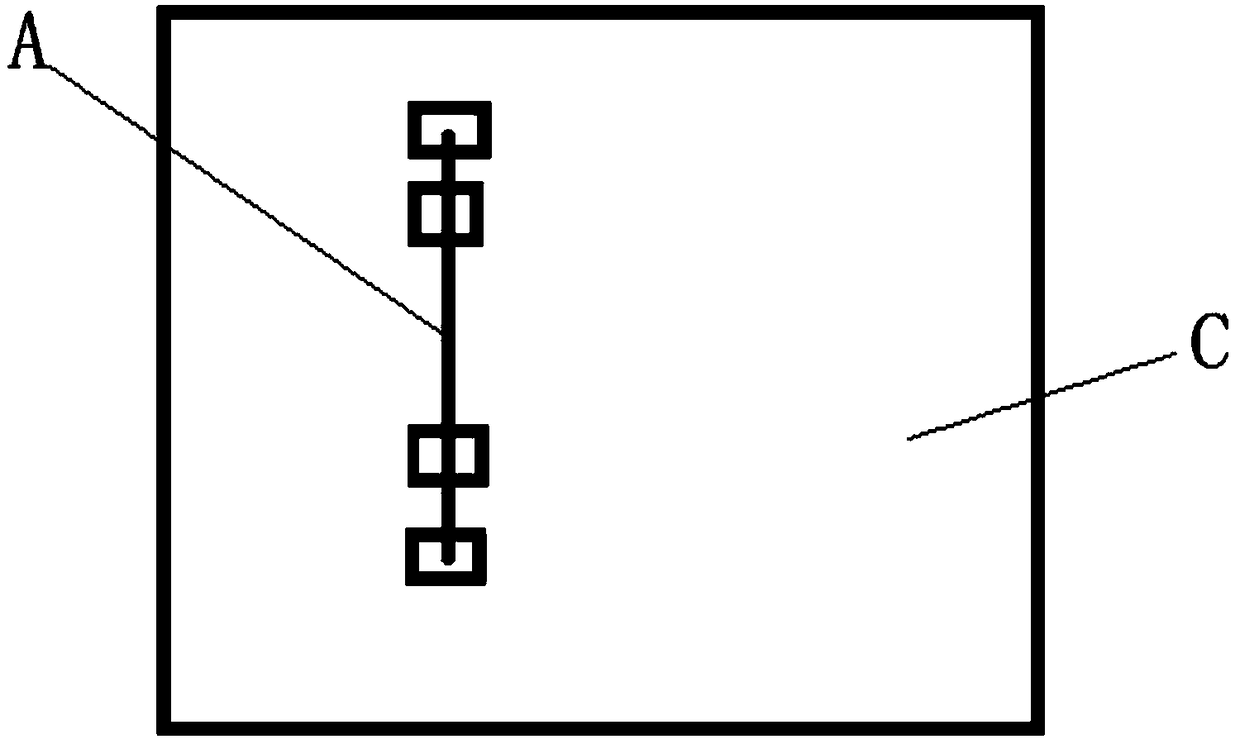
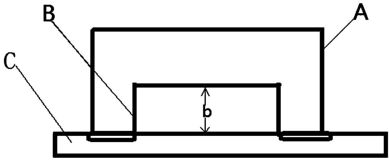
[0035] During the specific manufacture of the present invention, the horizontal and vertical distances and lengths between the first coupled inductance structure and the second coupled inductance structure (primary and secondary coils) are determined by the layout structure, inductance and coupling inductance coefficient during application, using three-dimensional electromagnetic field Simulation software aids design and implementation. Affected by integrated circuit devices and layout routing, often the metal coupling structure cannot be arranged in a regular shape to form the most reasonable positional relationship. The various embodiments of the present invention are only used as examples, and the influences of semiconductor devices and layout traces on the position and shape of the coupled inductor are ignored, and the description is made in principle. Theoretically, the structure of the present invention can bypass any semiconductor device and layout routing through the c...


PUM


Abstract

A coupling inductance structure for an integrated circuit is disclosed, At least two metal couple structures are use as inductors of transformer devices in integrate circuits, two ends of each metal coupling structure are respectively connected with metal layers on a semiconductor device substrate, and different coupling inductors are obtained between metal coupling structures through spatial positional relationship under the condition of satisfying integrated circuit process. The invention utilizes bonding wires bonded on the semiconductor device substrate to form the primary and secondary inductors of the transformer device, thereby avoiding the limitation of the metal layer process in the integrated circuit field. The coupling inductor can make full use of all the space in the integrated circuit layout to improve the chip area utilization. Primary and secondary inductors can be fabricated to adapt to the layout of the shape, as far as possible using the shape of the primary and secondary inductors to provide the best coupling mutual inductance.

Description

technical field [0001] The invention relates to the field of integrated circuits, in particular to a coupled inductance structure for integrated circuits. Background technique [0002] When manufacturing integrated circuit layout structures in the field of integrated circuits, balun devices or transformer devices are often used. A balun device or a transformer device usually realizes mutual inductance by coupling coils, and the common ones are lateral coupling mechanism and longitudinal (up and down) coupling mechanism. These two commonly used coupling mechanisms have the same disadvantages. The mutual induction coil is implemented using the metal layer of the semiconductor device, and the thickness and width of the coil are limited by the integrated circuit process. The thickness of the metal layer in the field of integrated circuits is generally less than 4 microns, and the width is less than 20 microns. The quality factor of the coupled inductance formed under the limit...

Claims


Application Information

Patent Timeline
IPC IPC(8): H01L23/64H01L23/49
Inventor 赵奂
Owner 格兰康希通信科技(上海)股份有限公司
Why Eureka
Try Eureka