Image sensor and manufacturing method thereof

A technology of image sensor and manufacturing method, applied in the field of image sensor, capable of solving problems such as large dark current, pixel optical crosstalk, etc.

Pending Publication Date: 2021-02-23
WUHAN XINXIN SEMICON MFG CO LTD
View PDF0 Cites 0 Cited by
  • Summary
  • Abstract
  • Description
  • Claims
  • Application Information

AI Technical Summary

Problems solved by technology

In practical applications, the vertical charge transfer image sensor has the problems of large dark current and optical crosstalk between pixels

Method used


Image

  • Image sensor and manufacturing method thereof
  • Image sensor and manufacturing method thereof
  • Image sensor and manufacturing method thereof

Examples


Embodiment Construction

[0036]Embodiments of the present invention provide an image sensor and a method of making it. The invention is further described in detail below with reference to the accompanying drawings and specific embodiments. The advantages and features of the present invention will be more clear depending on below. It should be noted that the accompanying drawings use a very simplified form and use non-precision ratios, which is intended to be convenient, and clearly assisted in explaining the purposes of the embodiments of the present invention.

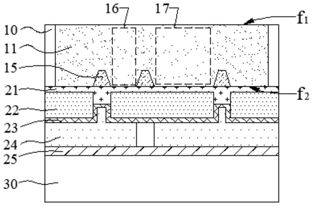
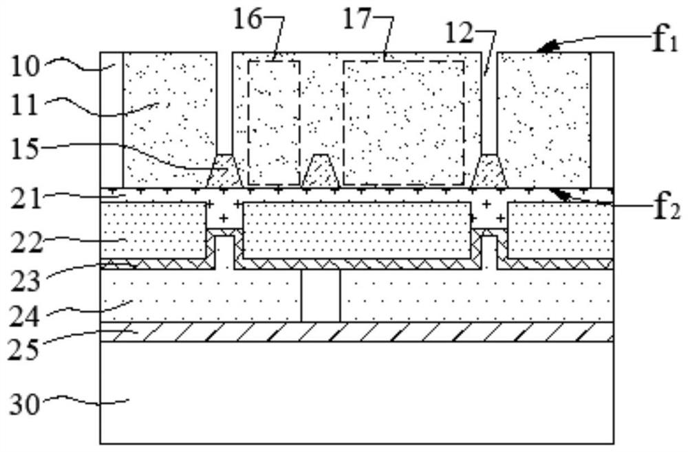
[0037]The embodiment of the present invention provides a method of making an image sensor, such asfigure 1 As shown, including:

[0038]A substrate is provided, and a plurality of pixel units are distributed on the substrate, and the pixel unit is located in a first type well region in the substrate;

[0039]The substrate is etched to form an isolation trench between adjacent pixel units;

[0040]The second type of ion implantation is performed on the peripher...


PUM

PropertyMeasurementUnit
widthaaaaaaaaaa

Abstract

The invention provides an image sensor and a manufacturing method thereof, and the method comprises the steps: providing a substrate, wherein a plurality of pixel units are distributed on the substrate, and the pixel units are located in a first-type well region in the substrate; etching the substrate to form an isolation trench located between the adjacent pixel units; performing ion implantationof a second type on the peripheral substrate of the isolation trench, wherein ions of the second type and ions in the first type well region form a PN junction; and enabling the isolation layer to beplaced in the isolation trench. Deep trench isolation (DTI) and PN junction isolation formed by ion implantation are combined through isolation between pixel units, PN junctions are formed in a peripheral substrate of an isolation trench, carriers generated due to defects near the isolation trench are prevented from freely entering a reading region and a photosensitive region, dark current is reduced, and meanwhile, good electrical and optical isolation effects are achieved; moreover, the area of the isolation region is reduced, and the chip area utilization rate of the image sensor is improved.

Description

Technical field[0001]The present invention belongs to the field of image sensors, and more particularly to an image sensor and a method of making it.Background technique[0002]Vertical Charge Transfer Image Sensor (VPS, Vertical CHARGE TRANSFERRING PIXELSENSORS) is a three-dimensional image sensor based on a standard flash process or a semiconductor image sensor based on a floating gate structure, that is, a floating gate (FG) structure to form an image sensor. Pixel units, by converting the intensity of the optical signals in which each pixel unit induced into the amount of electron number on the pixel unit floating gate layer, to realize the number of optical signals. It has the characteristics of high cell density, small cell size, etc. The working principle is to be coupled to the floating gate using the voltage generated by the optical electron of the photosensitive zone, thereby changing the transistor threshold voltage of the reading area, and implements image recognition. In ...

Claims


Application Information

Patent Timeline
Patent Type & Authority Applications(China)
IPC IPC(8): H01L27/146
CPCH01L27/14605H01L27/1463H01L27/14632H01L27/14643H01L27/14687
Inventor 鲁林芝施森华王同信
Owner WUHAN XINXIN SEMICON MFG CO LTD
Why Eureka
Try Eureka