Gallium nitride gate controlled tunneling bidirectional switching device

A bidirectional switching device and gallium nitride gate technology, which is applied in semiconductor devices, electrical components, circuits, etc., can solve the problems of device surface oxidation, process incompatibility, surface state generation, etc., and achieve low on-resistance and chip area utilization The effect of high rate and low power consumption

Inactive Publication Date: 2018-04-13
UNIV OF ELECTRONICS SCI & TECH OF CHINA +1
View PDF2 Cites 0 Cited by
  • Summary
  • Abstract
  • Description
  • Claims
  • Application Information

AI Technical Summary

Problems solved by technology

However, conventional gallium nitride bidirectional switching devices have ohmic contacts, require heavy metals such as gold, and are prepared under high temperature conditions, making the device incompatible with traditional silicon processes
And during the high-temperature ohmic annealing process, the surface of the device will be oxidized, which will lead to the generation of surface states
These surface traps trap electrons, resulting in a large dynamic resistance during dynamic switching of the device

Method used


Image

  • Gallium nitride gate controlled tunneling bidirectional switching device
  • Gallium nitride gate controlled tunneling bidirectional switching device
  • Gallium nitride gate controlled tunneling bidirectional switching device

Examples


Embodiment Construction

[0017] Below in conjunction with accompanying drawing, describe technical scheme of the present invention in detail:

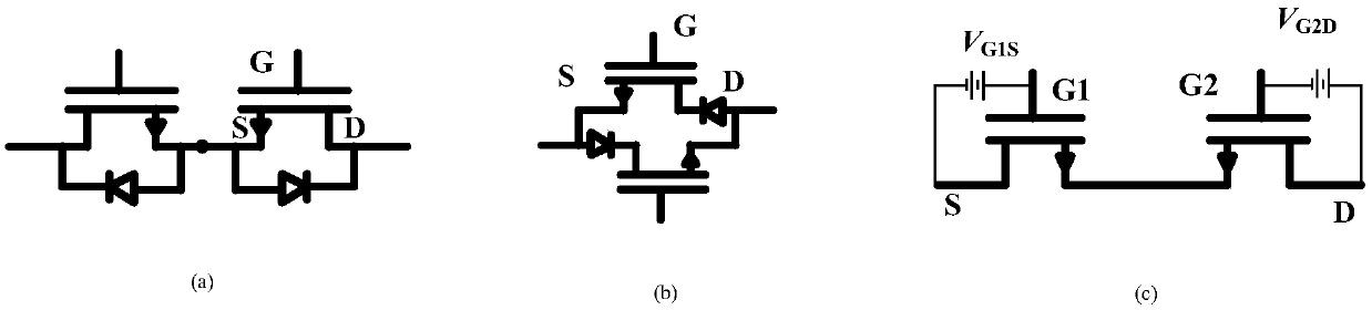
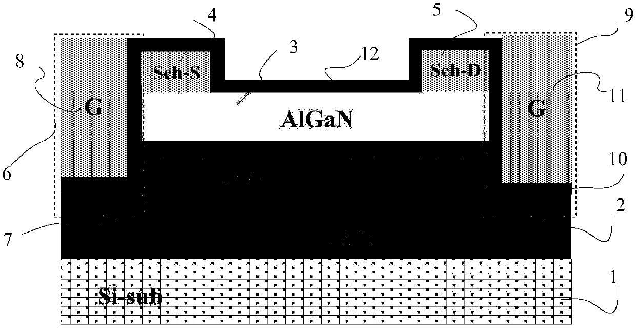
[0018] Such as figure 2 As shown, the gallium nitride gate-controlled tunneling bidirectional switch device of the present invention includes a substrate 1, a GaN layer 2, and an MGaN layer 3 that are sequentially stacked from bottom to top, and the GaN layer 2 and MGaN layer 3 form a heterojunction The two ends of the device are respectively a Schottky source structure 4 and a Schottky drain structure 5 formed by growing metal directly on the MGaN layer 3; the Schottky source structure 4 and Schottky drain structure 5 It is distributed symmetrically with the vertical center line of the device; there is an insulating deep groove gate structure (the first insulating deep groove gate structure 6 and the second Insulated deep groove gate structure 9); the two insulated deep groove gate structures are only separated by a gate dielectric from the Schottky source ...


PUM


Abstract

The invention relates to a gallium nitride gate controlled tunneling bidirectional switching device, belonging to the technical field of semiconductor power devices. The invention provides a gallium nitride gate controlled tunneling bidirectional switching device without ohmic contact, which can avoid a series of negative effects caused by high temperature ohmic annealing process. The working state of the device is changed by insulated gate structures near each Schottky contact controlling the energy band structure of the barrier layer below the Schottky contact, so as to realize the bidirectional conduction and bidirectional blocking capability of the gallium nitride gate controlled tunneling bidirectional switching device. Because the gallium nitride gate controlled tunneling bidirectional switching device does not have ohmic contact and does not need heavy metals, the technology of the gallium nitride gate controlled tunneling bidirectional switching device can be compatible with the traditional CMOS technology.

Description

technical field [0001] The invention belongs to the technical field of semiconductor power devices, in particular to a gallium nitride gate-controlled tunneling bidirectional switch device. Background technique [0002] Bidirectional switches with bidirectional conduction current and blocking voltage characteristics are widely used in motor drives, aircraft, AC power supply units, marine electric propulsion, and electric vehicles. The traditional bidirectional switch is composed of two insulated gate bipolar transistors (IGBT) and two power diodes in reverse series, the structure is similar to figure 1 (a), in such a structure, the current will flow through two different devices, and the longer current path will cause a larger turn-on voltage drop, which in turn will cause a higher power loss in the bidirectional switch. In order to reduce the conduction loss of bidirectional switches and improve system efficiency, bidirectional switches based on reverse resistance devices ...

Claims


Application Information

Patent Timeline
Patent Type & Authority Applications(China)
IPC IPC(8): H01L29/778H01L29/417H01L29/423H01L29/47H01L29/51
CPCH01L29/7786H01L29/41775H01L29/42316H01L29/475H01L29/517H01L29/518
Inventor 陈万军施宜军李茂林崔兴涛刘杰刘超周琦张波
Owner UNIV OF ELECTRONICS SCI & TECH OF CHINA
Why Eureka
Try Eureka