Array arrangement and transfer method and transfer device of Micro-LED substrate and display device

A technology of array arrangement and transfer method, which is applied in the directions of transportation and packaging, conveyor objects, electrical components, etc., can solve the problems of high cost of fine transfer head matrix, increase production cost, etc., achieve simple operation, improve transfer efficiency, reduce cost effect

Pending Publication Date: 2019-09-17
GUANGDONG UNIV OF TECH
View PDF0 Cites 5 Cited by
  • Summary
  • Abstract
  • Description
  • Claims
  • Application Information

AI Technical Summary

Problems solved by technology

However, it only transfers LEDs with asymmetrical top and bottom edges, and pre-designed molds must be used, and the key to this method is the loading film with densely arranged loading slots. In terms of its fine and accurate processing, the processing cost of the mold is also low. Not too low; or use a large number of transfer head matrix adsorption transfer, altho

Method used


Image

  • Array arrangement and transfer method and transfer device of Micro-LED substrate and display device
  • Array arrangement and transfer method and transfer device of Micro-LED substrate and display device
  • Array arrangement and transfer method and transfer device of Micro-LED substrate and display device

Examples


Embodiment Construction

[0038] In order to make the purposes, technical solutions and advantages of the embodiments of the present application clearer, the technical solutions in the embodiments of the present application will be clearly and completely described below in conjunction with the drawings in the embodiments of the present application. Obviously, the described embodiments It is a part of the embodiments of this application, not all of them. Based on the embodiments in this application, all other embodiments obtained by persons of ordinary skill in the art without making creative efforts belong to the scope of protection of this application.

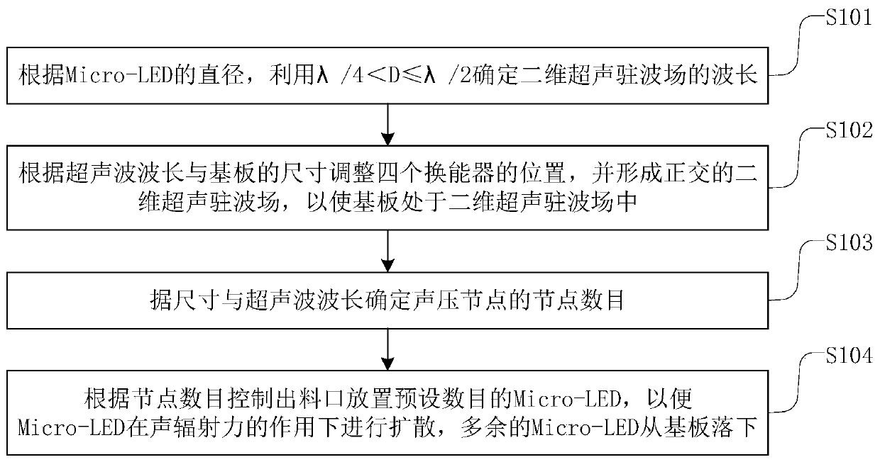
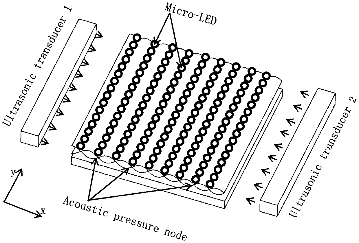
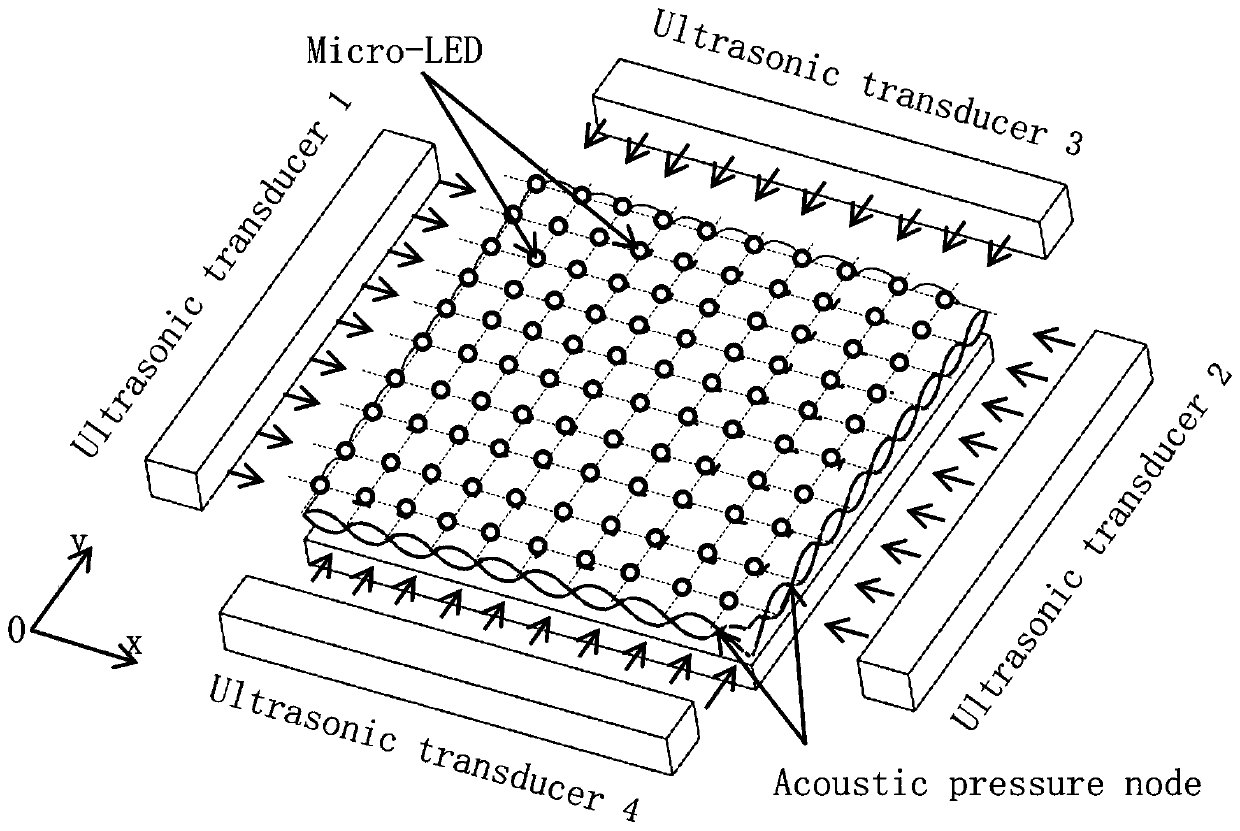
[0039]At present, the mass transfer method and device of Micro-LED require a large number of transfer head matrix or micro-groove matrix molds to realize the mass transfer of Micro-LED, but the production of these key molds will inevitably increase the production cost. Based on the above technical problems, this embodiment provides an array arrangemen...


PUM


Abstract

The invention discloses an array arrangement and transfer method of a Micro-LED substrate. The method comprises the following steps of: according to the diameter of a Micro-LED, determining the ultrasonic wave length of a two-dimensional ultrasonic standing wave field by utilizing lambda/4 < D <= lambda/2; adjusting the positions of four transducers according to the ultrasonic wave wavelength and the size of a substrate, and forming an orthogonal two-dimensional ultrasonic standing wave field above the substrate; determining the node number of sound pressure nodes according to the size and the ultrasonic wave wavelength; and controlling a discharging device to place a preset number of Micro-LEDs according to the number of the nodes, so that the Micro-LEDs are diffused under the action of acoustic radiation force, and redundant Micro-LEDs fall off from the substrate. Therefore, the Micro-LEDs are diffused and sorted under the action of the acoustic radiation force of the two-dimensional ultrasonic standing wave field, so that each Micro-LED occupies one acoustic pressure node, array arrangement and huge amount transfer are realized, the operation is simple, the transfer efficiency is improved, and the cost is reduced. The invention further provides a transfer device and a Micro-LED display device which both have the above beneficial effects.

Description

technical field [0001] The present application relates to the field of semiconductor technology, and in particular to a Micro-LED substrate (hereinafter referred to as Micro-LED) array arrangement transfer method, a Micro-LED substrate transfer device, and a Micro-LED display device. Background technique [0002] Micro-LED is a display technology that miniaturizes and matrixes the LED structure, and individually drives and addresses each pixel. Various indicators such as brightness, life, contrast, response time, energy consumption, viewing angle and resolution of micro light-emitting diodes are superior to LCD and OLED technologies, and are regarded as a new generation of display technology that can surpass OLED and traditional LEDs, but , due to the extremely high efficiency in the packaging process, the 99.9999% yield rate and the need for transfer accuracy within plus or minus 0.5μm; while the size of Micro-LED components is basically less than 50μm and the number is ten...

Claims


Application Information

Patent Timeline
IPC IPC(8): H01L21/02H01L21/677
CPCH01L21/02H01L21/677H01L21/67703
Inventor 陈新雷君君程峰纪轩荣袁懋诞陈燕
Owner GUANGDONG UNIV OF TECH
Why Eureka
Try Eureka