Circuit board based on fault discontinuous meshes and preparation process of circuit board
A technology for circuit boards and substrates, applied in the field of circuit boards based on fault-discontinuous meshes and its preparation process, can solve problems such as difficult to ensure the effective formation of partition layers and generation of bubbles, and achieve the elimination of transmission loss, accelerated fading, The effect of improving integrity
- Summary
- Abstract
- Description
- Claims
- Application Information
AI Technical Summary
Problems solved by technology
Method used
Image
Examples
Embodiment 1
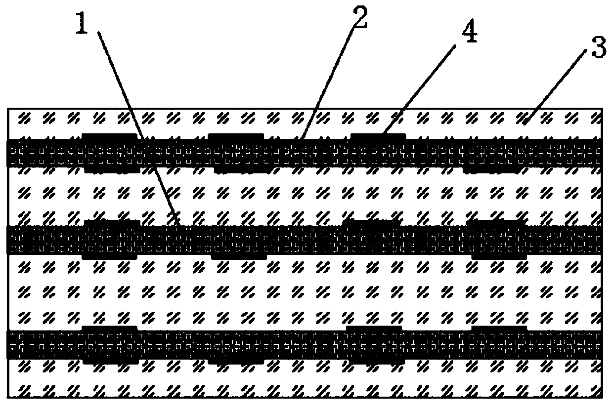
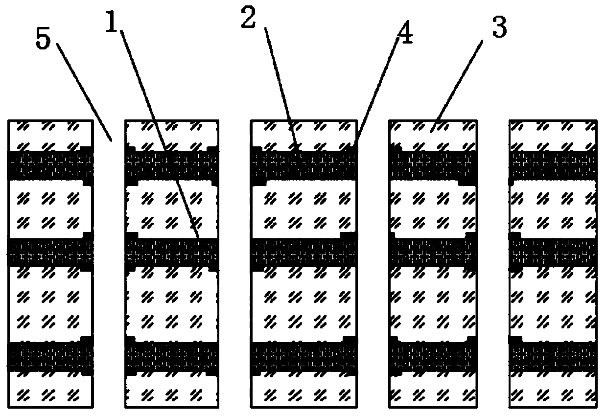
[0046] see figure 2 , a circuit board based on a fault-discontinuous mesh, including a first substrate 1 and a second substrate 2, the second substrate 2 is located on the upper side of the first substrate 1, and the second substrate 2 is connected to the first substrate 1 There is a connection piece 3, and the end of the second substrate 2 away from the first substrate 1 is also connected to the connection piece 3, and the connection between the first substrate 1 and the second substrate 2 and the connection piece 3 is connected with a plating resist 4, please refer to image 3 , the first substrate 1, the second substrate 2 and the connecting sheet 3 are correspondingly drilled with a plurality of through holes 5, please refer to Figure 4 , and the through hole 5 is located at the position of the plating resist layer 4 to set up the isolation layer region 6 .
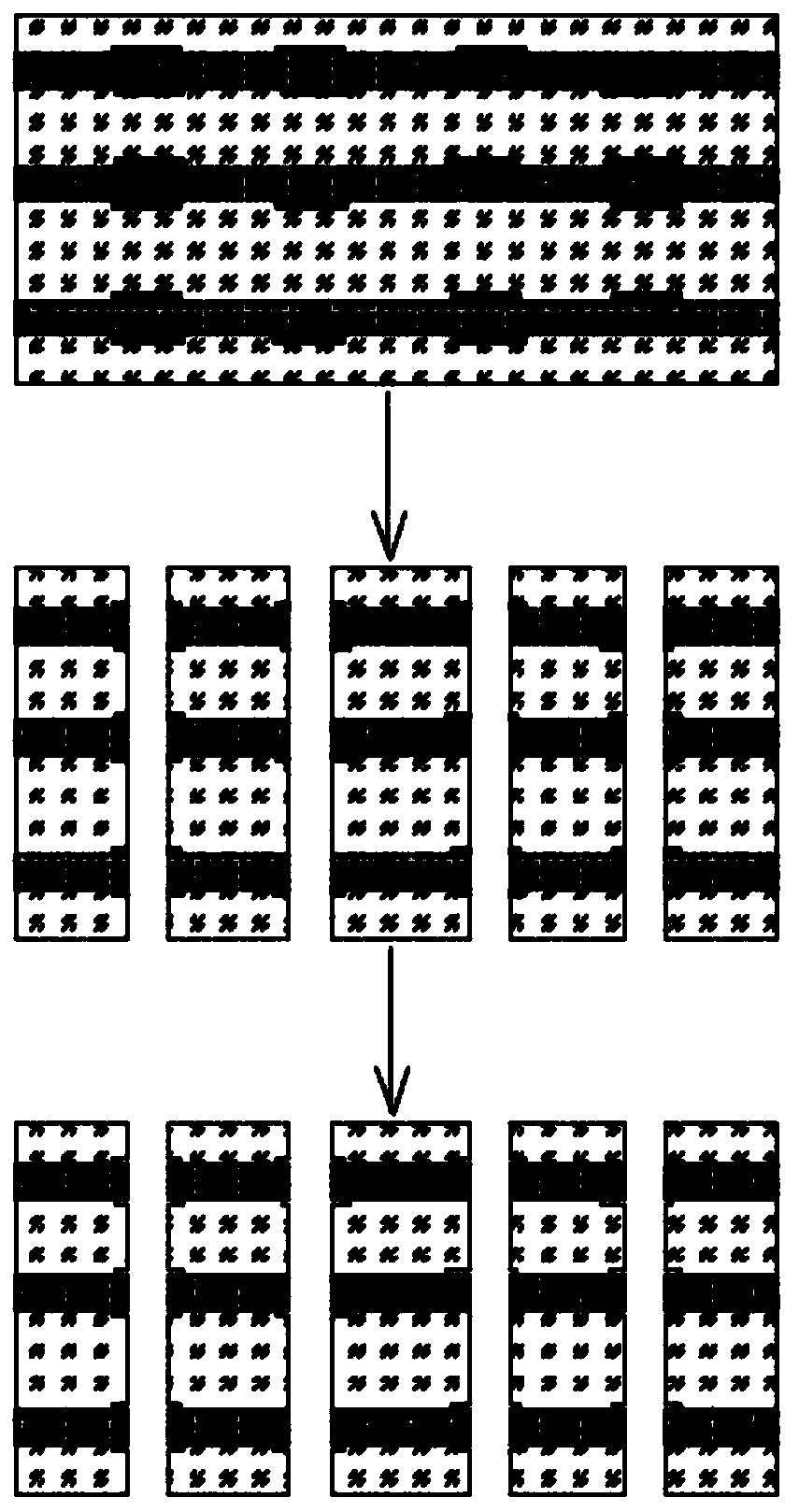
[0047] see figure 1 , a circuit board based on fault discontinuous mesh, its preparation process is:
[0048] ...
Embodiment 2
[0063] see figure 2 , a circuit board based on a fault-discontinuous mesh, including a first substrate 1 and a second substrate 2, the second substrate 2 is located on the upper side of the first substrate 1, and the second substrate 2 is connected to the first substrate 1 There is a connection piece 3, and the end of the second substrate 2 away from the first substrate 1 is also connected to the connection piece 3, and the connection between the first substrate 1 and the second substrate 2 and the connection piece 3 is connected with a plating resist 4, please refer to image 3 , the first substrate 1, the second substrate 2 and the connecting sheet 3 are correspondingly drilled with a plurality of through holes 5, please refer to Figure 4 , and the through hole 5 is located at the position of the plating resist layer 4 to set up the isolation layer region 6 .
[0064] see figure 1 , a circuit board based on fault discontinuous mesh, its preparation process is:
[0065] ...
PUM
 Abstract
Description
Claims
Application Information


