
A periodic crescent-shaped nano-gap array and its preparation method

A nano-gap and crescent-shaped technology, applied in nanotechnology, material excitation analysis, instruments, etc., can solve the problems of expensive instruments, limited applications, low throughput, etc., and achieve simple and easy operation, high controllability, and simple operation Effect

Active Publication Date: 2021-04-02
JILIN UNIV
View PDF9 Cites 0 Cited by
  • Summary
  • Abstract
  • Description
  • Claims
  • Application Information

AI Technical Summary

Problems solved by technology

[0003] However, there are very few precious metal nanostructures with gaps and tips at the same time, and electron beam etching and focused ion beam etching are usually used. These complex processes require expensive instruments, take a long time, and have low throughput. its further application

Method used


Image

  • A periodic crescent-shaped nano-gap array and its preparation method
  • A periodic crescent-shaped nano-gap array and its preparation method
  • A periodic crescent-shaped nano-gap array and its preparation method

Examples


Embodiment 1

[0036] Embodiment 1: the preparation of hydrophilic silicon substrate

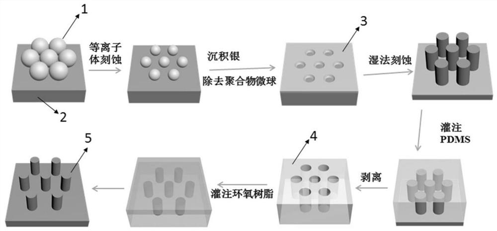
[0037] Cut the silicon wafer into 2×2cm with a glass knife 2 size, put it into a mixture of concentrated sulfuric acid (mass fraction 98%) and hydrogen peroxide (30%) (volume ratio is concentrated sulfuric acid: hydrogen peroxide = 7:3), heat to 80°C, keep for 5h and let it cool to room temperature , Rinse with a large amount of deionized water to obtain a hydrophilic silicon wafer, then rinse the silicon wafer with ethanol, blow dry with nitrogen, and use an oxygen plasma machine to clean the surface for 3 minutes to obtain a hydrophilic and uniform surface.

Embodiment 2

[0038] Embodiment 2: Preparation of hydrophobic polystyrene microspheres

[0039] At room temperature, add 3 mL of deionized water to 1 mL of 5 wt % polystyrene microsphere dispersion with a diameter of 700 nm, perform ultrasonication for 10 min, centrifuge at 8900 rpm for 10 min, absorb the supernatant, and re- 3 mL of deionized water was added for sonication and centrifugation was performed again, after which the process was repeated 4 times. After absorbing the supernatant for the last time, add 3 mL of a mixture of ethanol and deionized water (the volume ratio of ethanol: deionized water is 1:1) to the solid, centrifuge at 8900 rpm for 10 min, absorb the supernatant, and then Add 3mL of ethanol and deionized water mixture to the remaining solid matter, sonicate and centrifuge again, then repeat this process 8 times, after the last suction of the supernatant, put the remaining solid matter in an oven at 30 After drying for 8 hours, a mixture of ethanol and deionized water ...

Embodiment 3

[0040] Example 3: Preparation of hexagonal close-packed monolayer polystyrene colloidal crystals

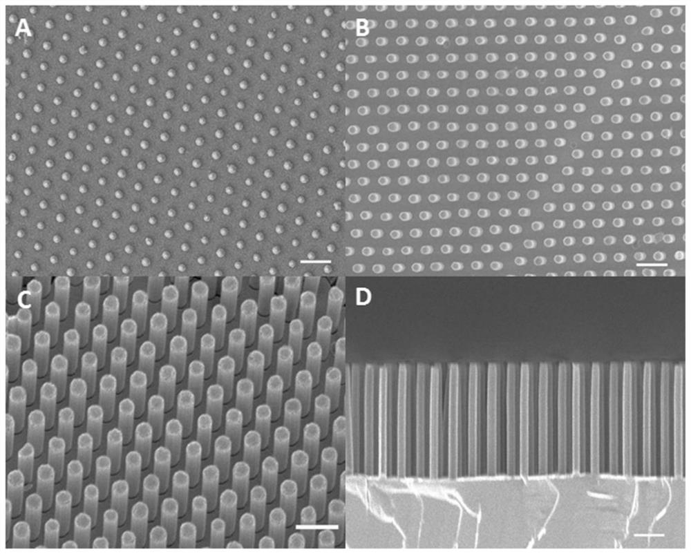
[0041] Use a disposable syringe to draw 0.2 mL of the ethanol and deionized water dispersion of hydrophobic polystyrene microspheres with a diameter of 700 nm prepared in Example 2, and use an instrument to slowly drop it onto the air-deionized water interface of the petri dish , add 80 μL of an aqueous solution of sodium lauryl sulfate with a mass concentration of 10wt% along the side of the petri dish, and let it stand for a while, and the polystyrene microspheres will form a single layer of hexagonal close-packed on the air-deionized water interface. form. Taking the hydrophilic silicon substrate obtained in Example 1 as an example, it is deep below the water surface, slowly lifted up from the bottom of the compact single-layer polystyrene microspheres, and placed on a filter paper with an inclined plane of 60° for natural drying, that is, on the silicon substrate. A monolaye...


PUM

PropertyMeasurementUnit
diameteraaaaaaaaaa
thicknessaaaaaaaaaa
pore sizeaaaaaaaaaa

Abstract

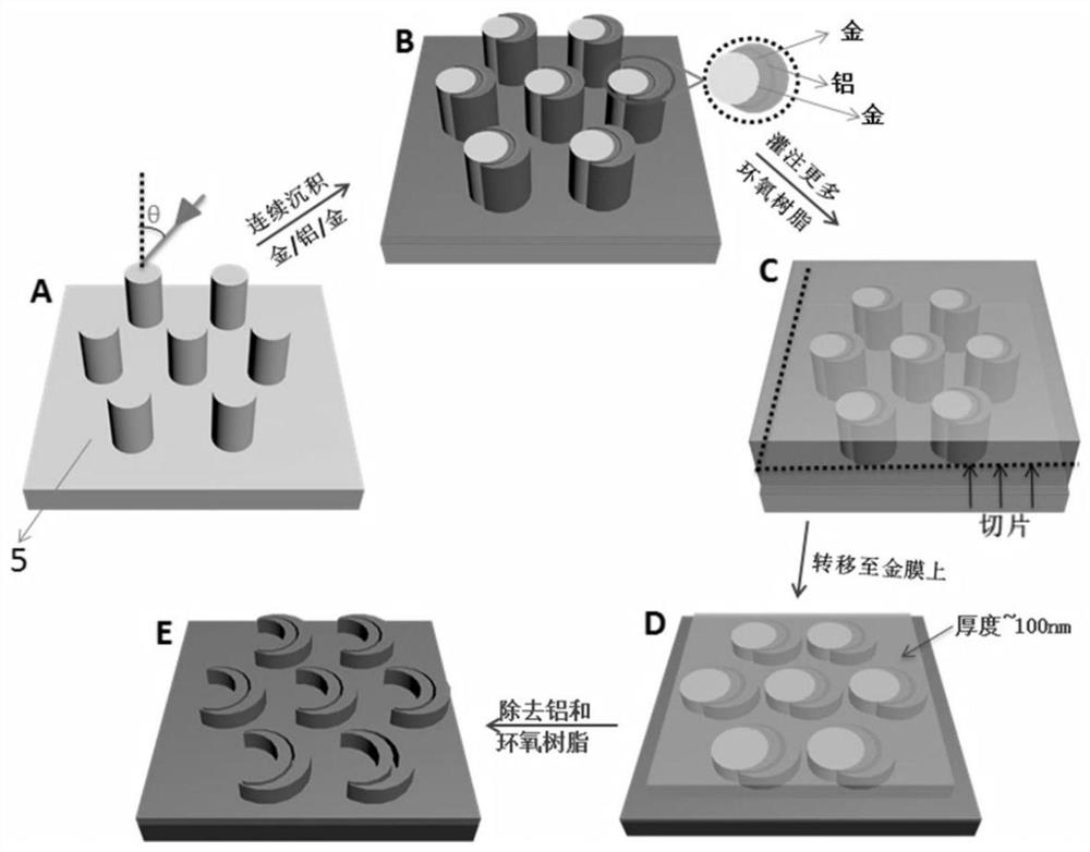
The invention relates to a regular crescent nanometer gap array with an improved surface enhanced Raman scattering performance and a preparation method of the array, and belongs to the technical field of surface enhanced Raman scattering. The preparation method relates to a colloid etching method, metal aided wet method etching, a physical vapor deposition method and a nanometer cutting method. The whole process is simple, highly controllable, and low in consumption, has no requirements for expensive instruments or an aseptic environment, and is universal. The etching time is controlled to prepare crescent nanometer gap arrays of different periods; the thickness of an intermediate layer is controlled to prepare the crescent nanometer gap arrays with different gap widths; multiple hot spots are coupled, the electromagnetic field of a structure is enhanced, the surface enhanced Raman scattering performance is improved, and the crescent nanometer gap array can have specific effects in the fields including plasma, nonlinear optics, single molecule detection, photoelectron and meta-materials.

Description

technical field [0001] The invention belongs to the technical field of surface-enhanced Raman scattering, and in particular relates to a periodic crescent-shaped nano-gap array with greatly improved surface-enhanced Raman scattering performance and a preparation method thereof. Background technique [0002] Surface-enhanced Raman scattering (SERS) structured films on substrates have attracted many people's attention because of their [1,2] , nonlinear optics [3] , single molecule detection [4,5] , Optoelectronics [6] and metamaterials [7] played an important role in other fields. a large number of adjacent nanoparticles [8] ,Nanowires [9] and some complex nanostructures [4-6] The gaps between them, or the nanostructures with tips all show good surface-enhanced Raman scattering performance. [0003] However, there are very few noble metal nanostructures with gaps and tips at the same time, and electron beam etching and focused ion beam etching are usually used. These c...

Claims


Application Information

Patent Timeline
Patent Type & Authority Patents(China)
IPC IPC(8): G01N21/65B82Y40/00
CPCB82Y40/00G01N21/658
Inventor 张刚张蔚
Owner JILIN UNIV
Learn More