Eureka AIR delivers breakthrough ideas for toughest innovation challenges, trusted by R&D personnel around the world.

Semiconductor device failure analysis method

A failure analysis and semiconductor technology, which is applied in the direction of single semiconductor device testing, instruments, measuring devices, etc., can solve the problem that the bias voltage cannot be applied to the test point, and achieve the effect of reducing manpower and time costs

Inactive Publication Date: 2019-09-20
YANGTZE MEMORY TECH CO LTD
View PDF6 Cites 2 Cited by
  • Summary
  • Abstract
  • Description
  • Claims
  • Application Information

AI Technical Summary

Problems solved by technology

[0005] In view of the above-mentioned shortcomings of the prior art, the purpose of the present invention is to provide a failure analysis method for semiconductor devices, which is used to solve the problem of inability to accurately and efficiently apply bias to the test points in the device during the CAFM test in the prior art. pressure problem

Method used


Image

  • Semiconductor device failure analysis method
  • Semiconductor device failure analysis method
  • Semiconductor device failure analysis method

Examples


Embodiment 1

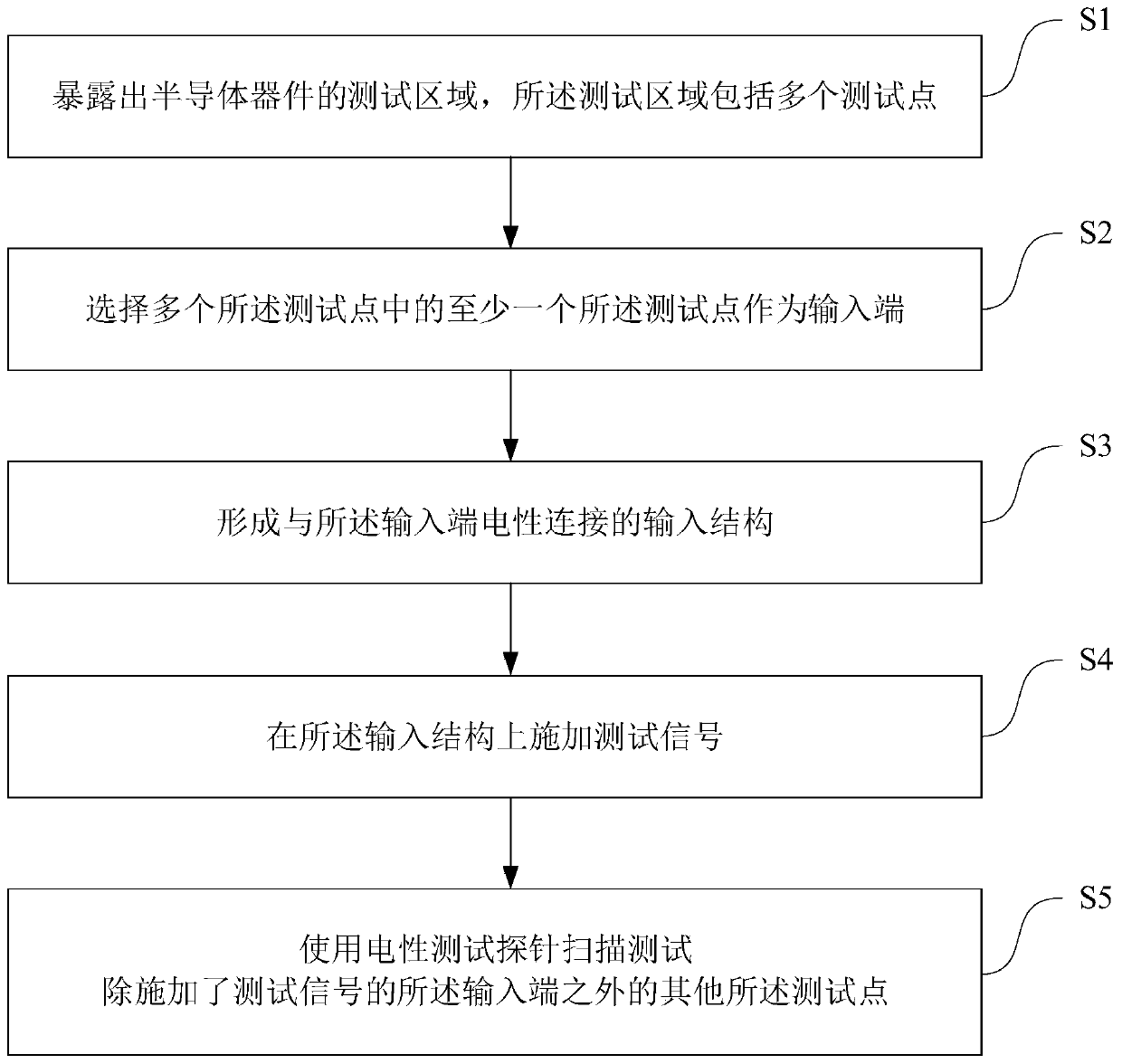
[0062] see Figure 1 to Figure 4 , the present embodiment provides a semiconductor device failure analysis method, comprising the following steps:

[0063] 1) Exposing the test area of ​​the semiconductor device, the test area includes a plurality of test points;

[0064] 2) selecting at least one of the multiple test points as an input terminal;

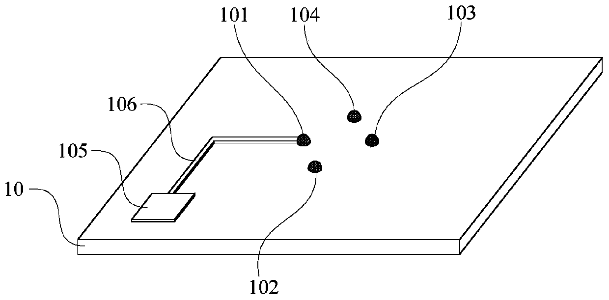
[0065] 3) forming an input structure electrically connected to the input end;

[0066] 4) applying a test signal on the input structure;

[0067]5) Use electrical test probes to scan and test the other test points except the input terminal to which the test signal is applied.

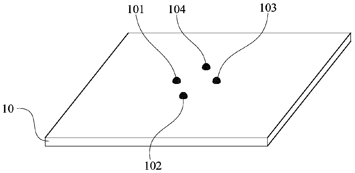
[0068] In step 1), if figure 1 S1 and figure 2 As shown, a test area 10 of a semiconductor device is exposed, and the test area 10 includes a plurality of test points. In this embodiment, the semiconductor device failure analysis method is used to test the leakage characteristics of the test point. There are four test points on the test area 10 of the...

Embodiment 2

[0076] see Figure 5 to Figure 9 , this embodiment provides a failure analysis method for a semiconductor device. Compared with the method in Embodiment 1, the difference of this embodiment is that all of the plurality of test points are used as the input terminals, and a plurality of the input terminals are formed to be electrically connected to the plurality of input terminals. input structures; applying a test signal to each of the input structures in turn, and using electrical test probes to scan and test other test points except the input terminals to which the test signals are applied. That is, this embodiment needs to test the leakage characteristics of each of the multiple test points and other test points.

[0077] As an example, such as Figure 5 to Figure 9 As shown, the four test points on the test area 20: the first test point 201, the second test point 202, the third test point 203 and the fourth test point 204 are all selected as input terminals, and test sign...


PUM


Abstract

The invention provides a semiconductor device failure analysis method. The method comprises the following steps of exposing a test area of a semiconductor device, wherein the test area includes a plurality of test points; selecting at least one of the plurality of test points as an input end; forming an input structure electrically connected to the input end; applying a test signal to the input structure; and using an electrical test probe to scan and test the test points except for the input end to which the test signal is applied. Through introducing the new semiconductor device failure analysis method, when a semiconductor device is tested and analyzed by using an electrical probe test method such as a conductive atomic force microscope and the like, input structures electrically connected to the test points are formed. A bias voltage is applied to the test points through the input structures and labor and time cost required for failure analysis can be effectively reduced through the multiple input structures.

Description

technical field [0001] The invention relates to the field of semiconductor integrated circuit manufacturing, in particular to a failure analysis method for semiconductor devices. Background technique [0002] As semiconductor devices continue to shrink in size and become more complex, new failure analysis techniques are emerging. Atomic Force Microscopy (AFM) can obtain nanoscale resolution by directly interacting with the sample surface by using a tiny needle tip. Among them, the conductive atomic force microscope (Conductive Atomic Force Microscopy, CAFM) can scan and analyze the current signal of the nanoscale area on the sample surface by introducing a conductive probe. This has broad application prospects in the field of electrical failure analysis such as semiconductor device leakage. [0003] At present, in the process of using CAFM to analyze the leakage of semiconductor devices, it is generally used to apply a bias voltage to the substrate of the sample and use CA...

Claims


Application Information

Patent Timeline
Patent Type & Authority Applications(China)
IPC IPC(8): G01R31/26G01Q60/24G01Q30/20
CPCG01Q30/20G01Q60/24G01R31/2601
Inventor 高慧敏魏磊张顺勇
Owner YANGTZE MEMORY TECH CO LTD
Why Eureka
Eureka Blog
Learn More