Test structure and manufacturing method thereof

A technology for testing structures and manufacturing methods, used in semiconductor/solid-state device manufacturing, electrical components, and electrical solid-state devices, etc., and can solve problems such as device short-circuits, incorrect contact of electrical wiring, and incorrect contact of metal filling layers.

Inactive Publication Date: 2019-09-24
WUHAN XINXIN SEMICON MFG CO LTD
View PDF4 Cites 0 Cited by
  • Summary
  • Abstract
  • Description
  • Claims
  • Application Information

AI Technical Summary

Problems solved by technology

However, this method is prone to circuit reliability problems, such as wrong contact between electrical connections, or wrong contact between metal filling layers in via holes, which may cause short circuits in the device

Method used


Image

  • Test structure and manufacturing method thereof
  • Test structure and manufacturing method thereof
  • Test structure and manufacturing method thereof

Examples


Embodiment Construction

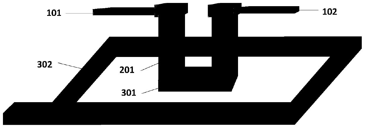
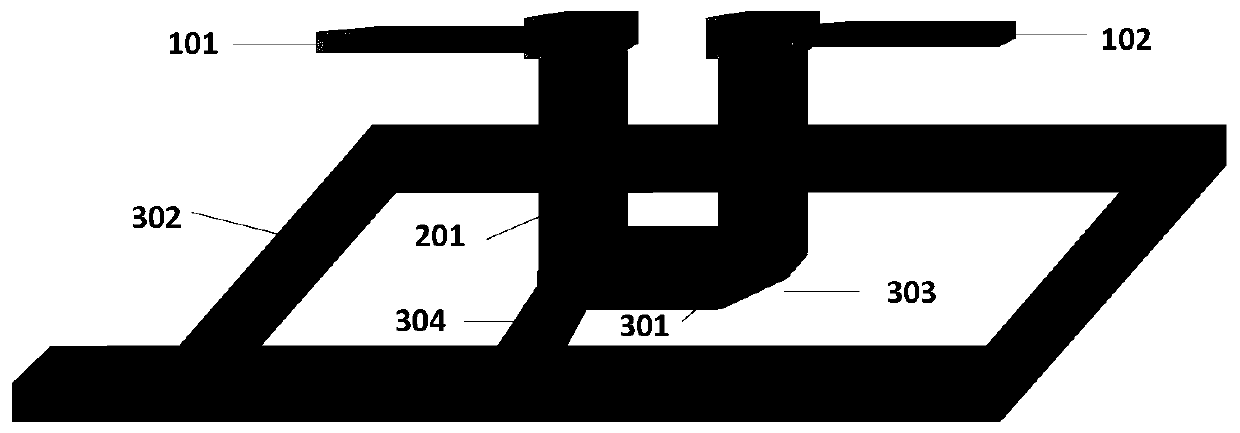
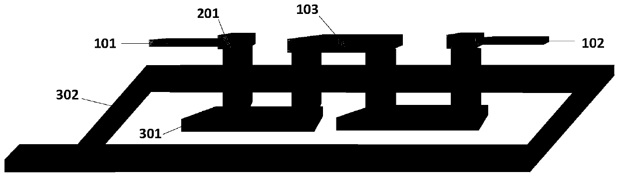
[0045] In order to make the above-mentioned purpose, features and advantages of the present application more obvious and understandable, the specific implementation manners of the present application will be described in detail below in conjunction with the accompanying drawings.

[0046] In the following description, a lot of specific details are set forth in order to fully understand the application, but the application can also be implemented in other ways different from those described here, and those skilled in the art can do it without violating the content of the application. By analogy, the present application is therefore not limited by the specific embodiments disclosed below.

[0047] Secondly, the present application is described in detail in conjunction with schematic diagrams. When describing the embodiments of the present application in detail, for the convenience of explanation, the cross-sectional view showing the device structure will not be partially enlarged...


PUM


Abstract

The invention provides a test structure and a manufacturing method thereof. The test structure comprises a first test line, a second test line, a first input end and a second input end. The first test line is used for establishing electrical connection between first metal filling layers in the plurality of first through holes, the first input end and the second input end are electrically connected through the first test line and the plurality of first metal filling layers, the second test line is connected with the second metal filling layers in the second through holes, and the second test line is grounded. Therefore, after a voltage is applied to the first input end and the second input end, a leakage current can be detected in the second test line when a short-circuit fault happens between the first test line and the second test line, or between the first through hole and the second through hole, or between the first test line and the second through hole, or between the second test line and the first through hole, so that the reliability of a circuit with a plurality of through holes is monitored at the same time. Therefore, the monitoring is more comprehensive, and the monitoring efficiency is also improved.

Description

technical field [0001] The present application relates to the field of semiconductor devices and its manufacture, in particular to a test structure and its manufacturing method. Background technique [0002] With the continuous development of semiconductor technology, 3D-IC (three-dimensional integrated circuit) technology has been widely used. It uses wafer-level packaging technology to stack and bond wafers with different functions. This technology has high performance and low cost. With the advantages of cost and high integration, the formed three-dimensional integrated circuit has smaller size and power consumption, and can realize more functions. Therefore, 3D-IC technology has broad application prospects, and has become the key direction of integrated circuit development in recent years. [0003] In the implementation of wafer-level packaging technology, different wafers can be bonded through the intermolecular chemical bonding (bonding) technology of the bonding laye...

Claims


Application Information

Patent Timeline
Patent Type & Authority Applications(China)
IPC IPC(8): H01L23/544H01L21/48H01L23/48
CPCH01L21/4814H01L23/481H01L23/544
Inventor 单法宪
Owner WUHAN XINXIN SEMICON MFG CO LTD
Why Eureka
Try Eureka