
WAT test device, preparation method and test method for detecting metal connection uplift

A technology of metal connection and test device, which is applied in the field of WAT test device for detecting metal connection bulge, and can solve problems such as process problems and the like

Active Publication Date: 2021-01-29
SHANGHAI HUAHONG GRACE SEMICON MFG CORP
View PDF13 Cites 0 Cited by
  • Summary
  • Abstract
  • Description
  • Claims
  • Application Information

AI Technical Summary

Problems solved by technology

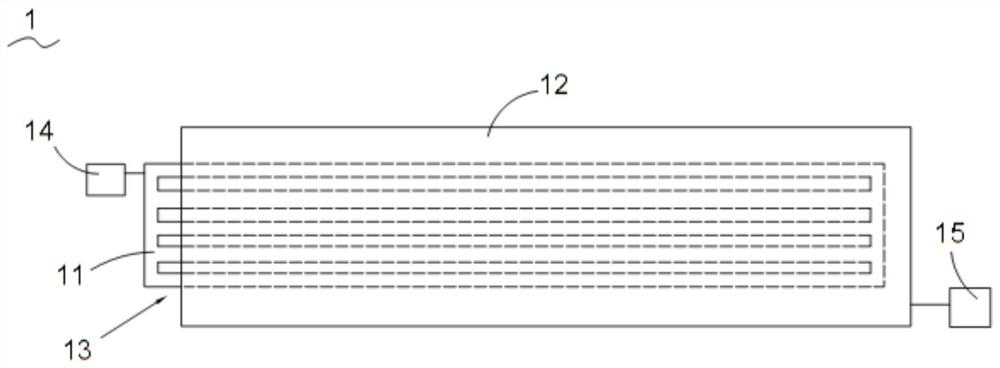
[0005] The first purpose of the present invention is aimed at the prior art, when the thickness of the dielectric is comparable to the height of the metal bump (Hillock) defect, the interlayer dielectric planarization process (IMD CMP) will inevitably grind the interlayer dielectric layer through and contact The bump (Hillock) defect to the front layer metal will cause a series of process problems and other defects. Provide a WAT ​​test device for detecting metal wiring bumps
[0006] The second object of the present invention is aimed at the prior art, when the thickness of the medium is comparable to the height of the metal bump (Hillock) defect, the interlayer dielectric planarization process (IMD CMP) is bound to grind and penetrate the interlayer dielectric layer and contact The bump (Hillock) defect to the front layer metal will cause a series of process problems and other defects. Provide a test method for the WAT test device used to detect the bump of the metal connection.
[0007] The third object of the present invention is aimed at the prior art, when the thickness of the dielectric is comparable to the height of the metal bump (Hillock) defect, the interlayer dielectric planarization process (IMD CMP) will inevitably grind the interlayer dielectric layer through and contact To the front-layer metal bump (Hillock) defect, which will cause a series of process problems and other defects Provide a method for preparing a WAT ​​test device for detecting metal wiring bumps

Method used


Image

  • WAT test device, preparation method and test method for detecting metal connection uplift
  • WAT test device, preparation method and test method for detecting metal connection uplift
  • WAT test device, preparation method and test method for detecting metal connection uplift

Examples


preparation example Construction

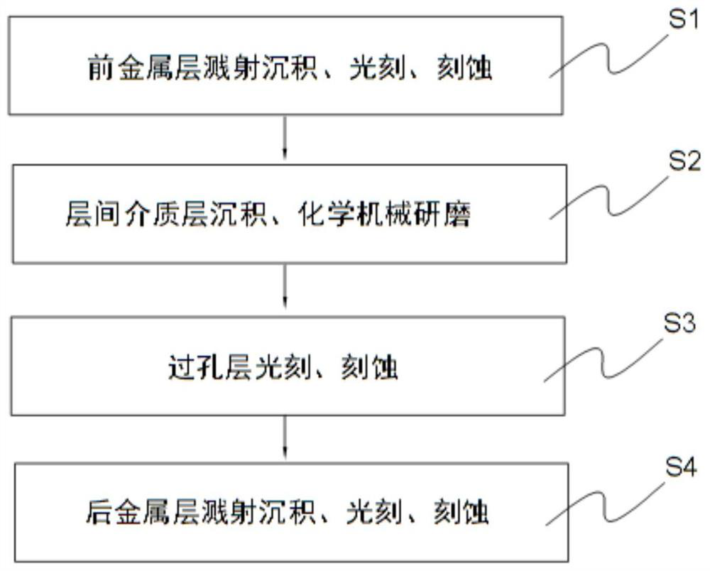
[0034] see figure 2 , figure 2 Shown is the flow chart of the preparation method of the WAT test device for detecting metal wire bumps according to the present invention. The preparation method of the WAT testing device 1 for detecting metal connection uplift includes:

[0035] Executing step S1: sputtering deposition of the front metal layer 11, photolithography, etching;

[0036] Executing step S2: deposition of interlayer dielectric layer 13, chemical mechanical polishing;

[0037]Executing step S3: photolithography and etching of the via layer;

[0038] Step S4 is performed: sputtering deposition, photolithography, and etching of the back metal layer 12 .

[0039] In order to reveal the technical solution of the present invention more intuitively and highlight the beneficial effects of the present invention, the structure and working principle of the WAT test device 1 for detecting metal connection bulge described in the present invention are described in conjunction...

no. 1 approach

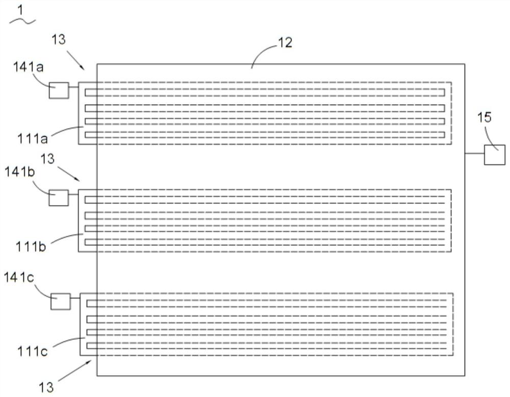
[0041] As a first embodiment of the present invention, non-limiting enumeration, for example, the WAT test device 1 for detecting metal wiring bumps includes a front metal layer 11, and the front metal layer 11 has a first preset line width The metal line 111a of the second preset line width, the metal line 111b of the second preset line width, and the metal line 111c of the third preset line width.

[0042] see image 3 , image 3 Shown is a schematic structural view of a WAT ​​testing device for detecting metal wire bumps according to the first embodiment of the present invention. The WAT test device 1 for detecting metal wiring bumps includes a front metal layer 11 and a back metal layer 12, the front metal layer 11 has a metal line 111a with a first preset line width, a second preset line width The metal line 111b of the metal line 111b of the third preset line width, and the interlayer dielectric layer 13 is set between the front metal layer 11 and the back metal layer ...

no. 2 approach

[0048] As a second embodiment of the present invention, non-limiting enumeration, for example, the WAT test device 1 for detecting metal wiring bumps includes a front metal layer 11, and the front metal layer 11 has a fourth preset line width The metal line 112a of the fifth predetermined line width and the metal line 112b of the fifth preset line width. Wherein, the fourth predetermined line width of the metal line 112a of the front metal layer 11 and the fifth predetermined line width of the metal line 112b of the front metal layer 11 are the most concerned metal line widths in the semiconductor device manufacturing process.

[0049] see Figure 4 , Figure 4 Shown is a schematic structural diagram of a WAT ​​testing device for detecting metal wire bumps according to the second embodiment of the present invention. The WAT test device 1 for detecting metal wiring bumps includes a front metal layer 11 and a back metal layer 12, the front metal layer 11 has a metal line 112a ...


PUM

PropertyMeasurementUnit
widthaaaaaaaaaa

Abstract

The invention discloses a WAT test device for detecting metal connecting line hillocks, a preparation method and a test method. The WAT test device for detecting metal connecting line hillocks includes a front metal layer and a rear metal layer. The front metal layer has at least one metal line of a predetermined line width. An interlayer dielectric layer is disposed between the front metal layerand the rear metal layers. The metal line of the predetermined line width of the front metal layer is electrically connected to a first test pad. The rear metal layer is electrically connected to a second test pad. The WAT test device for detecting metal connecting line hillocks can monitor the dependence of the metal connecting line hillocks on metal line width, and obtains a key metal line widthto provide a basis for a layout rule. In addition, the WAT test device for detecting metal connecting line hillocks can also monitor the reliability of the interlayer dielectric layer, such as TDDB.

Description

technical field [0001] The invention relates to the technical field of semiconductor manufacturing, in particular to a WAT ​​test device, a preparation method and a test method for detecting metal connection bumps. Background technique [0002] As the product process continues to shrink, the thickness of the back-end Inter Metal Dielectric (IMD) will continue to decrease. When the thickness of the medium is comparable to the height of the metal bump (Hillock) defect, the inter-layer dielectric planarization process (IMD) CMP) will inevitably grind and penetrate the interlayer dielectric layer and contact the bump (Hillock) defect of the front layer metal, which will cause a series of process problems, such as the grinding liquid (CMP Slurry) corrodes the front layer metal to form a void (Metal Void ), and subsequent metal deposition, such as through-hole titanium, through-hole titanium nitride, through-hole tungsten, etc., enter the cavity, thereby causing a short circuit be...

Claims


Application Information

Patent Timeline
Patent Type & Authority Patents(China)
IPC IPC(8): H01L21/66
Inventor 王卉
Owner SHANGHAI HUAHONG GRACE SEMICON MFG CORP
Learn More