Supercharge Your Innovation With Domain-Expert AI Agents!

Wafer Acceptance Test Pattern for Source Via Resistance of Flash Memory

A wafer acceptance test, source-side technology, applied in electronic circuit testing, semiconductor/solid-state device testing/measurement, circuits, etc., can solve the problem of inaccurate monitoring of electrical parameters, and achieve the effect of accurate monitoring

Active Publication Date: 2020-11-24
SHANGHAI HUALI INTEGRATED CIRCUIT CORP
View PDF5 Cites 0 Cited by
  • Summary
  • Abstract
  • Description
  • Claims
  • Application Information

AI Technical Summary

Problems solved by technology

[0003] However, there are many defects in the current electrical parameter monitoring methods, which lead to inaccurate monitoring of electrical parameters.

Method used


Image

  • Wafer Acceptance Test Pattern for Source Via Resistance of Flash Memory
  • Wafer Acceptance Test Pattern for Source Via Resistance of Flash Memory
  • Wafer Acceptance Test Pattern for Source Via Resistance of Flash Memory

Examples


Embodiment Construction

[0031] The technical solutions in the present invention will be clearly and completely described below in conjunction with the accompanying drawings. Apparently, the described embodiments are part of the embodiments of the present invention, not all of them. Based on the embodiments of the present invention, all other embodiments obtained by persons of ordinary skill in the art without making creative efforts belong to the protection scope of the present invention.

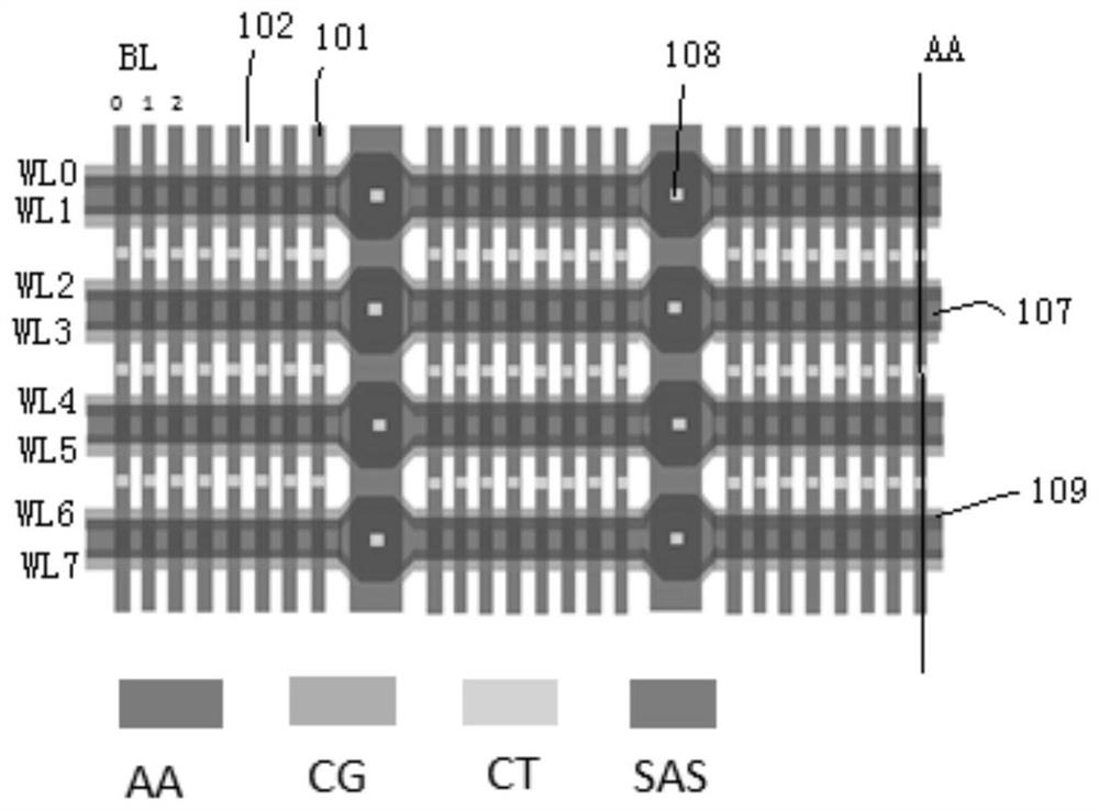
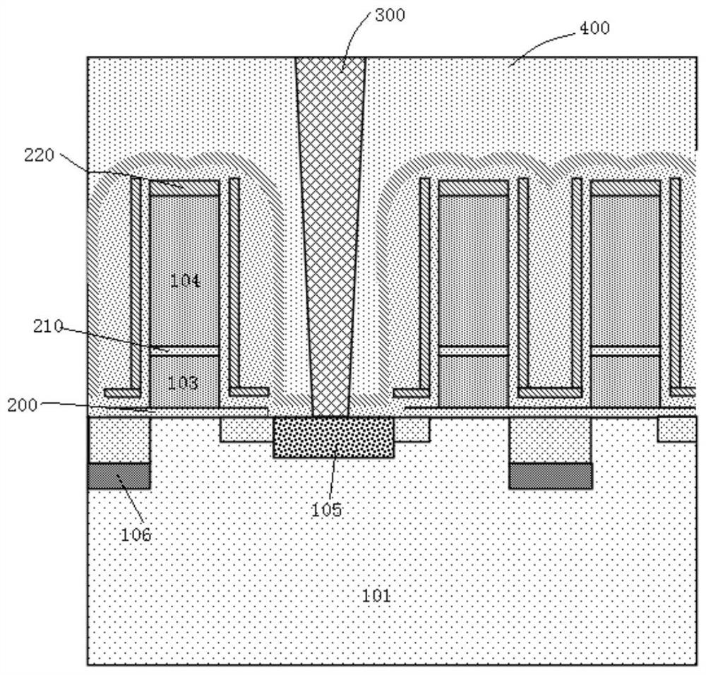
[0032] see figure 1 and figure 2 , figure 1 is a layout diagram of a flash memory, figure 2 is along figure 1 Schematic diagram of the cross-sectional structure of the AA line. Specifically, combine figure 1 and figure 2As shown, the flash memory is formed in the chip area, including a substrate, such as a silicon substrate, and the substrate includes a field oxygen isolation region 102 such as a shallow trench isolation region, and a plurality of active regions 101 isolated by the field oxygen isolation ...


PUM


Abstract

The invention relates to a wafer acceptable quality level test pattern of the source-terminal via resistance of a flash memory, and relates to a semiconductor integrated circuit. By designing, in the wafer acceptable quality level test pattern of the source-terminal via resistor of the flash memory, a source region row line connected to an active region and the field oxygen and a disconnection structure of the source region row line on a semiconductor substrate, an electrical connection path is formed by a source-terminal via, a source region row line and a connection metal layer to form the source-terminal via resistance test structure, thereby truly simulating the complex structure of a flash cell including AA / CG / SAS / CT / M1 so as to accurately monitor the resistance of a source-terminal via hole on the flash cell.

Description

technical field [0001] The invention relates to a semiconductor integrated circuit, in particular to a wafer acceptance test pattern of the source end via hole resistance of a flash memory. Background technique [0002] In semiconductor integrated circuits, with the development of semiconductor technology, the market share of non-volatile flash memory is getting higher and higher. In order to meet the market demands of high density, high performance, and low cost, technology nodes are getting smaller and smaller. The monitoring requirements for electrical parameters of non-volatile flash memory are more comprehensive, and the test is required to be more accurate, so as to better reflect the process conditions, such as the monitoring of via resistance in flash memory. [0003] However, there are many defects in the current electrical parameter monitoring methods, which lead to inaccurate monitoring of electrical parameters. Contents of the invention [0004] The object of...

Claims


Application Information

Patent Timeline
Patent Type & Authority Patents(China)
IPC IPC(8): H01L23/544G01R31/28
CPCG01R31/2851G01R31/2884G01R31/2898H01L22/32
Inventor 张金霜邹荣王奇伟陈昊瑜
Owner SHANGHAI HUALI INTEGRATED CIRCUIT CORP
Features
  • R&D
  • Intellectual Property
  • Life Sciences
  • Materials
  • Tech Scout
  • Unparalleled Data Quality
  • Higher Quality Content
  • 60% Fewer Hallucinations
Learn More