Supercharge Your Innovation With Domain-Expert AI Agents!

Testing method for polycrystalline silicon thin film resistor on polycrystalline silicon array substrate

A polysilicon thin film and array substrate technology, which is applied in the measurement of resistance/reactance/impedance, semiconductor/solid-state device testing/measurement, circuits, etc., can solve the damage of the substrate film layer, cannot accurately reflect the quality of polysilicon thin film, and the measurement method cannot be accurate and Non-destructive polysilicon thin film resistance testing and other issues to achieve the effect of reducing production loss and improving production efficiency

Inactive Publication Date: 2014-09-03
BOE TECH GRP CO LTD
View PDF4 Cites 0 Cited by
  • Summary
  • Abstract
  • Description
  • Claims
  • Application Information

AI Technical Summary

Problems solved by technology

[0004] Existing measurement methods cannot accurately and non-destructively test the resistance of polysilicon thin films on polysilicon array substrates
In the prior art, the resistance value estimated by the thickness is only a theoretical calculation value, which is usually quite different from the actual value. The resistance value calculated by the I-V curve is the resistance of the source and drain of the device, which is generally the total of multi-layer films including polysilicon films. The resistance of the polysilicon film cannot accurately reflect the quality of the polysilicon film; and other methods of directly measuring the resistance of the polysilicon film, such as the four-probe method, will cause damage to the substrate film (mainly the polysilicon film)

Method used


Image

  • Testing method for polycrystalline silicon thin film resistor on polycrystalline silicon array substrate
  • Testing method for polycrystalline silicon thin film resistor on polycrystalline silicon array substrate
  • Testing method for polycrystalline silicon thin film resistor on polycrystalline silicon array substrate

Examples


Embodiment 1

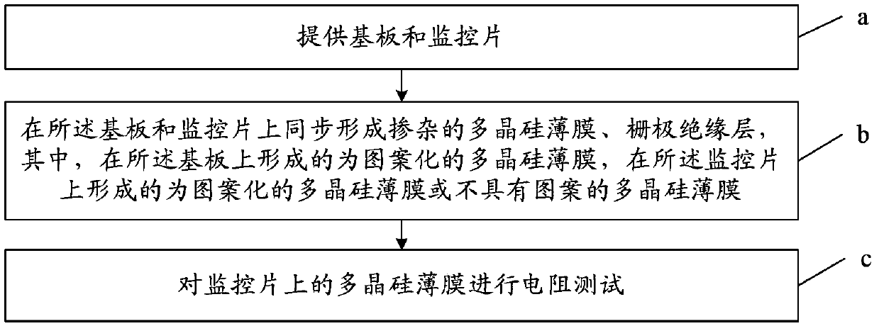
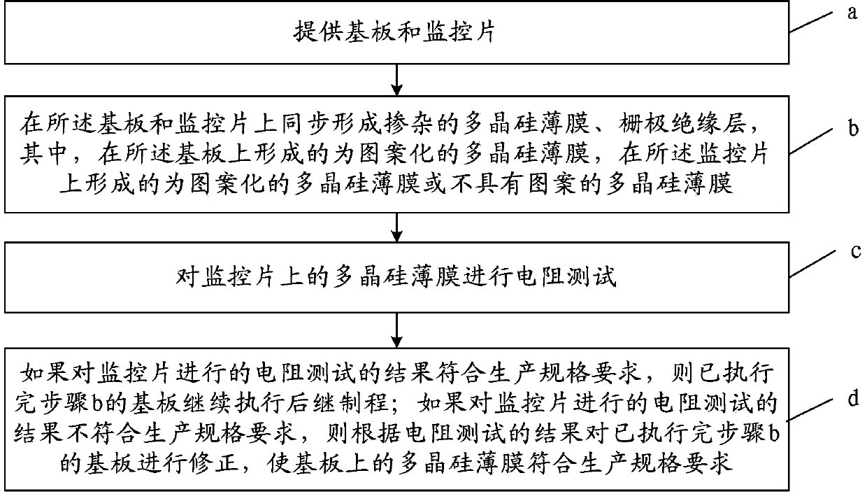
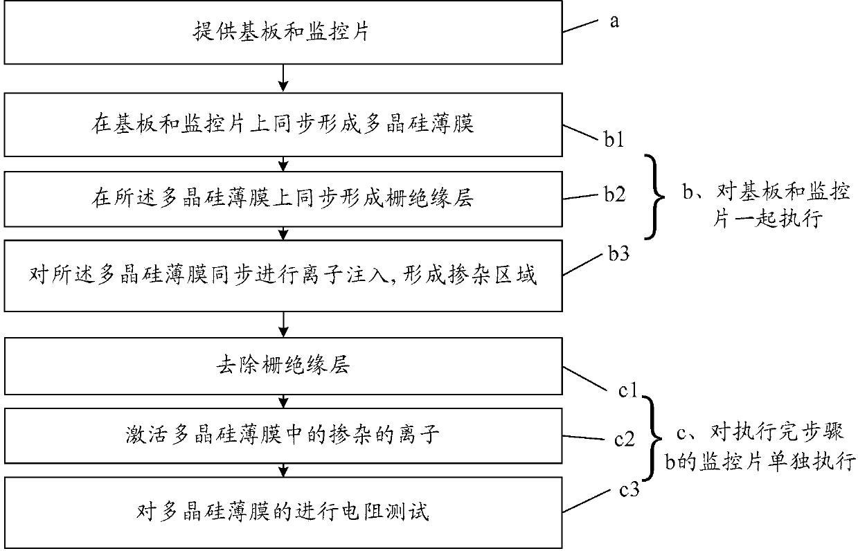
[0041] An embodiment of the present invention provides a method for testing polysilicon thin film resistance on a polysilicon array substrate, such as figure 1 As shown, the method includes:

[0042] a. Provide the substrate and monitor sheet;

[0043] b. Synchronously forming a doped polysilicon thin film and a gate insulating layer on the substrate and the monitor sheet, wherein the patterned polysilicon thin film is formed on the substrate, and the patterned polysilicon film is formed on the monitor sheet thin film or unpatterned polysilicon thin film;

[0044] c. Conducting a resistance test on the polysilicon film on the monitor sheet.

[0045] The specific number of the monitor sheets can be set according to production requirements, which is not limited in this embodiment. Since the material of the substrate has an influence on the composition, structure and quality of the film layer formed thereon, it is preferable that the monitor sheet is made of the same material ...


PUM

PropertyMeasurementUnit
thicknessaaaaaaaaaa

Abstract

Disclosed is a method for testing the resistance of a polysilicon thin film on a polysilicon array substrate, so as to timely and accurately monitor the resistance of a doped polysilicon thin film, thereby reducing production losses and improving production efficiency. The method comprises: providing a substrate and a monitoring piece; forming a doped polysilicon thin film and a gate insulation layer on the substrate and the monitoring piece synchronously, a patterned polysilicon thin film being formed on the substrate, and a patterned polysilicon thin film or a non-patterned polysilicon thin film is formed on the monitoring piece; performing a resistance test on the polysilicon thin film on the monitoring piece.

Description

technical field [0001] The invention relates to the field of semiconductors, in particular to a method for testing polysilicon thin film resistance on a polysilicon array substrate. Background technique [0002] The main feature of a Thin Film Transistor Liquid Crystal Display (TFT-LCD) is that each pixel is equipped with a semiconductor switching device, that is, a Thin Film Transistor (TFT). Therefore, in the TFT-LCD manufacturing process, the most important step is to form a TFT array on a substrate (preparing a polysilicon array substrate). Specifically, a polysilicon film is first formed on the substrate, and then the polysilicon film is doped to form the source and drain of the TFT device, and the resistance and resistance uniformity of the polysilicon film at the source and drain directly affect the electrical performance of the transistor device, and the polysilicon film The electrical conductivity of the polysilicon film is not only related to the dopant dose, but ...

Claims


Application Information

Patent Timeline
Patent Type & Authority Patents(China)
IPC IPC(8): G01R27/02
CPCH01L22/14G01R31/2637
Inventor 田慧金馝奭龙春平
Owner BOE TECH GRP CO LTD
Features
  • R&D
  • Intellectual Property
  • Life Sciences
  • Materials
  • Tech Scout
  • Unparalleled Data Quality
  • Higher Quality Content
  • 60% Fewer Hallucinations
Learn More