

Input interface circuit
A technology of input interface circuit and input terminal, applied in the direction of logic circuit, logic circuit connection/interface layout, electrical components, etc., can solve problems such as voltage VIN uncertainty
- Summary
- Abstract
- Description
- Claims
- Application Information
AI Technical Summary
Problems solved by technology
Method used
Image

Examples
Embodiment Construction
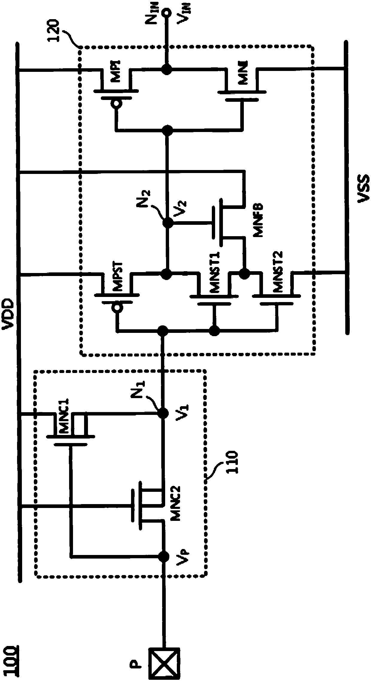
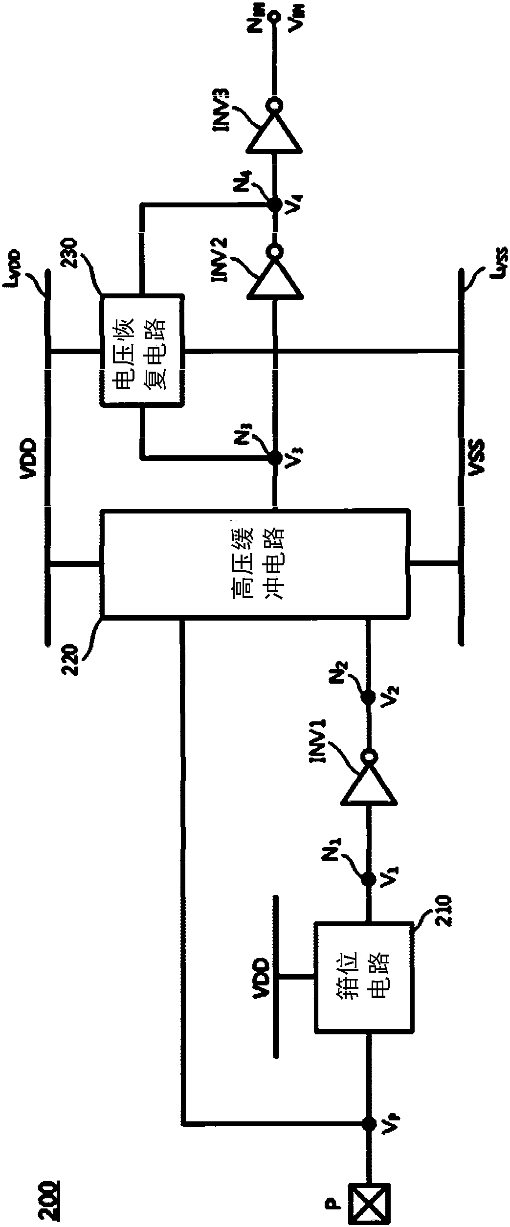
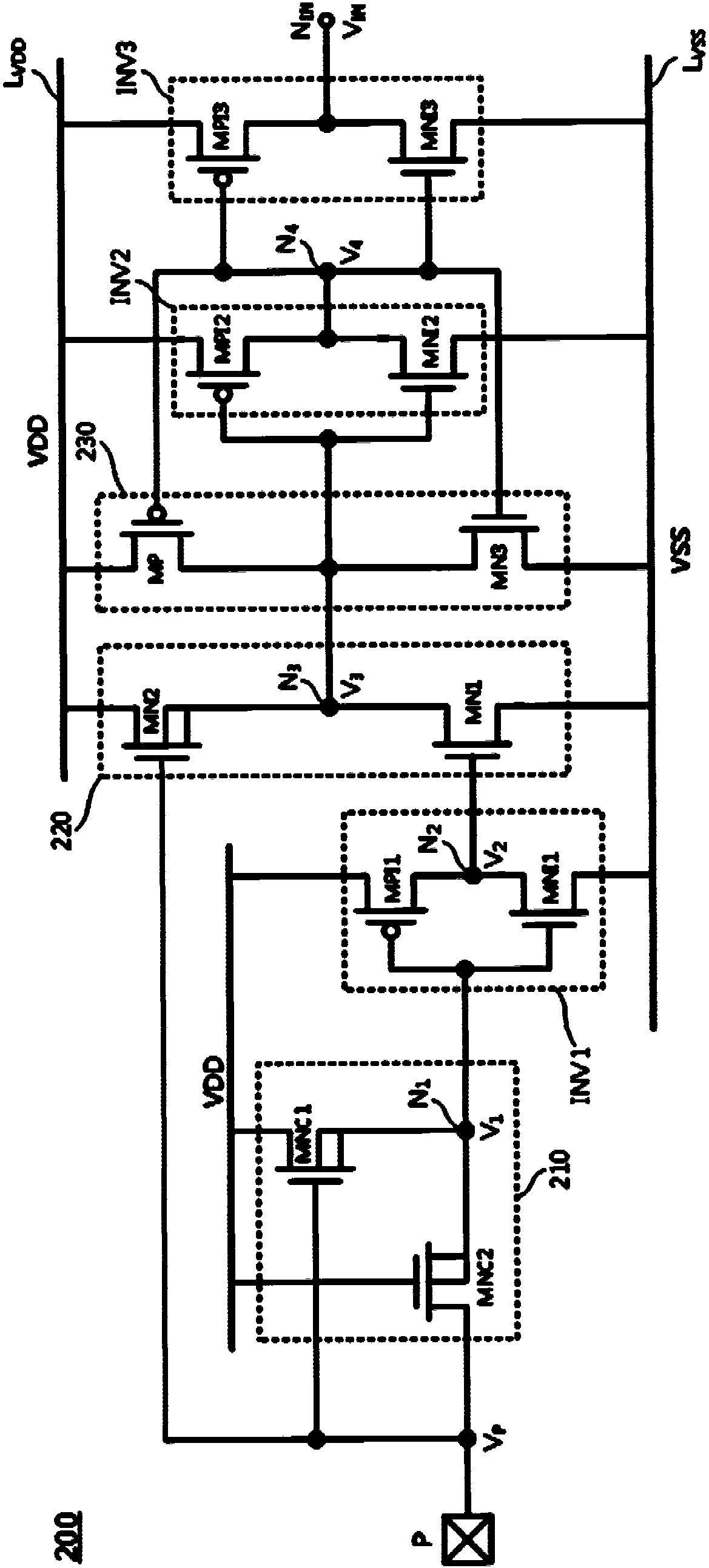
[0042] An embodiment according to the present invention is an input interface circuit, the functional block diagram of which is shown in figure 2 . The preset operating voltage of the input interface circuit 200 is represented by the symbol VDD, and its input pad P may receive a voltage (hereinafter referred to as the pad voltage V P ) ranges from zero to 2*VDD, and the voltage at its ground terminal is represented by the symbol VSS in the figure. In addition, the following symbol V TH Indicates the threshold voltage of N-type transistors in this process. Practically, the input interface circuit 200 can be integrated into various integrated circuit chips that need to receive digital signals twice the preset operating voltage. Such as figure 2 As shown, the input interface circuit 200 includes a power line L VDD , a ground wire L VSS , an input pad P, a clamping circuit 210 , a high voltage buffer circuit 220 , a voltage recovery circuit 230 , and three inverters INV1 -...
PUM
 Abstract
Description
Claims
Application Information