
A kind of LED point light source based on graphene/zno nanowire/p-gan film and preparation method thereof

A nanowire and graphene technology, applied in the field of semiconductor optics, can solve the problems affecting the electroluminescence performance of the heterojunction, and achieve the effect of reducing the size, enhancing the luminous intensity and large contact area

Active Publication Date: 2020-11-03
PEKING UNIV
View PDF8 Cites 0 Cited by
  • Summary
  • Abstract
  • Description
  • Claims
  • Application Information

AI Technical Summary

Problems solved by technology

This process involves ion etching, which inevitably causes great damage to the ZnO rods, thus affecting the electroluminescence performance of the heterojunction.

Method used


Image

  • A kind of LED point light source based on graphene/zno nanowire/p-gan film and preparation method thereof
  • A kind of LED point light source based on graphene/zno nanowire/p-gan film and preparation method thereof
  • A kind of LED point light source based on graphene/zno nanowire/p-gan film and preparation method thereof

Examples


Embodiment Construction

[0043] The present invention will be further elaborated below through specific embodiments in conjunction with the accompanying drawings.

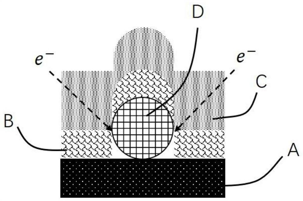
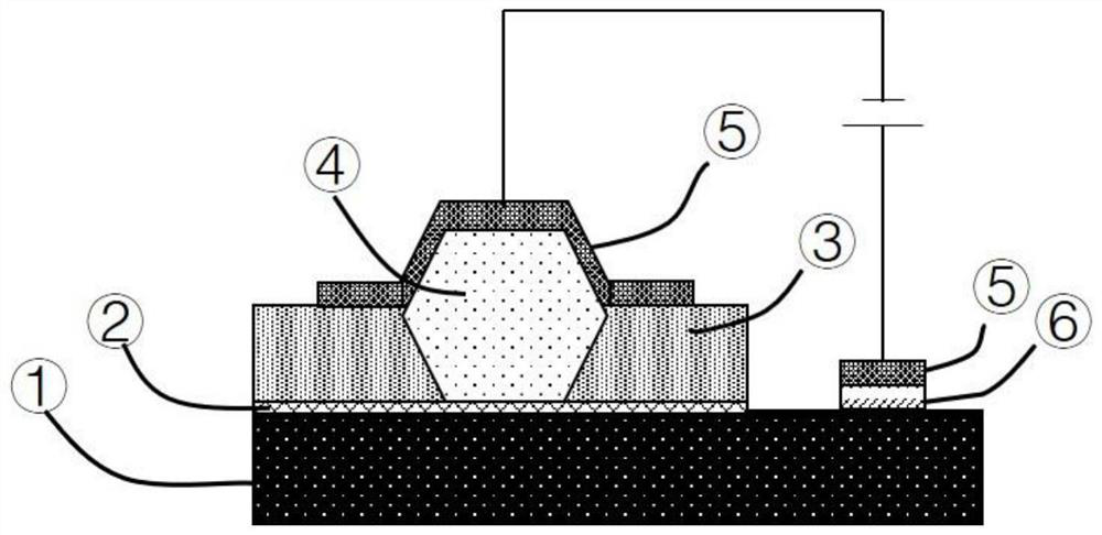
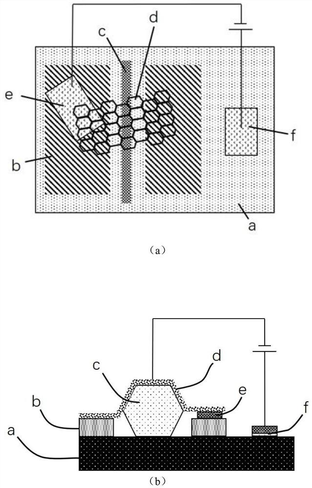
[0044] Such as image 3 and 4 As shown, the LED point light source based on the vertical structure of graphene / single ZnO nanowire / p-GaN film in this embodiment includes: growth substrate, p-GaN film layer a, positive electrode f, insulating layer b, groove , ZnO nanowire c, negative electrode e, and single-layer graphene d; wherein, a Mg-doped p-GaN film layer a with a thickness of about 1.75 μm is formed on the growth substrate, and the p-GaN film layer completely covers the growth substrate ; On the p-GaN thin film layer, a positive electrode f of Ni (10nm) / Au (50nm) is provided; on the p-GaN thin film layer, a thickness of about 100nm Al is formed except for the positive electrode 2 o 3 Insulating layer b, the insulating layer covers part of the p-GaN film layer except the positive electrode; a groove is arranged on the insulating l...


PUM

PropertyMeasurementUnit
diameteraaaaaaaaaa
widthaaaaaaaaaa
thicknessaaaaaaaaaa

Abstract

The invention discloses an LED point light source based on graphene / ZnO nanowire / P-GaN film, and a preparation method thereof. The LED point light source comprises a growth substrate, a P-GaN film layer, a positive electrode, an insulation layer, a groove, a ZnO nanowire, a negative electrode and a single-layer graphene; a single ZnO nanowire is placed in the groove on the P-GaN film layer to forma ZnO nanowire / P-GaN heterojunction; and, the single-layer graphene covers on the ZnO nanowire and the negative electrode. The contact area between the single-layer graphene and the ZnO nanowire is large, so as to increase the carrier injection area and improve the injection efficiency; and at the same time, the ZnO nanowire is not damaged by the device produced by the method, so that the luminous efficiency is greatly improved. The nanoscale point light source is formed on one end of the ZnO nanowire, so that the size of the photoelectronic device is effectively reduced; and thus, the LED point light source provided by the invention is widely applied to the fields of precise monolithic integration of the photoelectronic device, ultrahigh resolution biomedicine, supercapacitor informationstorage, and so on.

Description

technical field [0001] The invention relates to the field of semiconductor optics, in particular to an LED point light source based on a graphene / single ZnO nanowire / p-GaN film vertical structure and a preparation method thereof. Background technique [0002] Zinc oxide (ZnO) is a II-VI direct bandgap semiconductor with a forbidden band width of 3.37eV, a large exciton binding energy (60meV) at room temperature, a low growth temperature, and stable chemical properties. When its size is nanoscale, it often exhibits unique photoactivity, electrical activity and catalytic activity, and these properties have important application prospects in the field of optoelectronic devices. Because p-ZnO is difficult to synthesize, p-GaN, which is also a wurtzite structure, is often used in devices to contact ZnO to form a heterojunction. Gallium nitride (GaN) is a group III-V direct bandgap semiconductor with a forbidden band width of 3.39eV, which is often used in blue light emitting or ...

Claims


Application Information

Patent Timeline
Patent Type & Authority Patents(China)
IPC IPC(8): H01L33/14H01L33/24H01L33/26H01L33/38H01L33/00B82Y20/00B82Y40/00
CPCB82Y20/00B82Y40/00H01L33/005H01L33/0095H01L33/14H01L33/24H01L33/26H01L33/38
Inventor 林芳廖志敏廖馨
Owner PEKING UNIV
Learn More